Chemical State Analyses by Soft X-ray Emission Spectroscopy
JEOL NEWS Vol.53 No.5
Masami Terauchi and Yohei Sato
Center for Advanced Microscopy and Spectroscopy, Institute of Multidisciplinary Research for Advanced Materials, Tohoku University
A metallization of Si-sp3 network of Na8Si46 and a chemical state distribution in Na-doped CaB6, were observed by using a commercial EPMA-SXES instrument. Information observed in L-emission of 3d transition metal elements obtained by an original SEM-SXES instrument is discussed.
Introduction
For developing functional nano-scale materials and nano-scale devices, microscopic analysis and its feedback to manufacturing process is a key issue for those developments. For that purpose, analysis methods based on electron microscopy are crucial. Especially, spectroscopy methods give us fruitful information related to material’s functions. X-ray spectroscopy for elemental analysis may be the most widely used one. There are two types of energy-dispersive spectroscopy (EDS) and wavelength-dispersive spectroscopy (WDS). Electron energy-loss spectroscopy (EELS) and cathodoluminescence (CL, related to transition a in Fig. 1) are also widely used. Recently, a new face of soft X-ray emission spectroscopy (SXES), which can give electronic structure information, comes into a group of commercial methods [1, 2].
For investigating electronic structures related to material’s functions, EELS based on transmission electron microscopy (TEM) is widely used because of its better energy resolution than those of EDS and WDS and a wide energy range of 1-1000 eV. EELS can examine a dielectric property from a valence electron excitation spectrum (excitation b in Fig. 1). Especially, recent commercialization of a monochromator instrument realized one nanometer probe with an energy resolution of 0.1 eV or better. It enables us to analyze near-infrared property of industrial nano-particles [3] and also thermal lattice-vibrations [4]. Analysis of inner-shell excitation spectrum (excitation c in Fig. 1) combined with theoretical simulations becomes familiar for evaluating a relation between an electronic structure and a local crystal structure. Although EELS gives many information on electronic structure from a nm-scale specimen area, it cannot gives information of bonding electrons (valence bands). It can be realized by SXES, which analyzes X-ray emission energies of electronic transitions d in Fig. 1 with an energy-resolution better than 1 eV. SXES instruments for electron microscopy had been developed for TEM [5]. Because of a low detection efficiency of the method, it was commercialized as an instrument for electron probe microanalyzer (EPMA) and scanning electron microscope (SEM) which can use a larger probe current than that of TEM. As X-ray emissions for elemental analysis (EDS, WDS) are dominantly due to electronic transitions between inner-shell levels (transition e in Fig. 1), those spectra do not include information on valence electrons.
Fig. 1
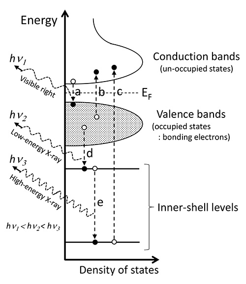
Schematic diagram of electronic transitions related to cathodoluminescence (a), valence electron excitation of EELS (b), inner-shell excitation spectrum of EELS (c), X-ray emission including valence electron information (d) and X-ray emission mainly used for elemental analysis (e).
A SXES instrument was first developed for a TEM [6]. The main bottle neck for application was a low detection efficiency. In high spacial resolution analysis of thin specimen by TEM, a specimen volume examined is small and an acquisition time of some tens of minutes or more is necessary for obtaining a reasonable signal to noise ratio. When applying this method to EPMA and SEM, an acquisition time of one or a few minutes is usual due to a larger beam current and a larger examination volume. This SXES method may be useful as a spectroscopy method for bulk materials as TEM-EELS method for thin specimens. Then, this EPMA/SEM-SXES can make a quick feedback to material processing.
When combining an inner-shell excitation EELS spectrum (probing unoccupied states) and a soft X-ray emission spectrum (probing occupied states), a whole electronic states can be figured out. Furthermore, an electronic excitation spectrum can be derived from a valence electron excitation EELS spectrum by using Kramers-Kronig analysis. Therefore, electron microscopy can analyze not only crystal structure and constituent elements but also a whole electronic structure of identified small specimen areas [5, 7].
In this manuscript, SXES observations on a metallization of Si-sp3 network of Na8Si46, a chemical state distribution in Na-doped CaB6, and information on L-emission of 3d transition metal elements are described.
Instruments and experimental condition
SXES instruments used in this report are shown in Fig. 2(a) EPMA (JEOL JXA-8230) attached with a commercial SXES spectrometer system (SS-94000SXES) and (b) SEM (JEOL JSM-6480LV) attached with our original spectrometer. Both SXES instruments are WDS type spectrometers based on flat-field grazing incidence optics by using aberration corrected gratings.
The commercial SXES instrument with two gratings can detect from 50 eV to 210 eV for 1st order spectrum, up to 420 eV for 2nd order spectrum, and much further for higher order spectrum. Actually, this spectrometer can detect soft X-ray emission signals of more than 70 elements [8]. Present data was measured by using a grating of JS200N with an averaged groove density of 1200 lines/mm. Detector is a back-thin type CCD. Energy resolution evaluated for a sharp Fermi edge structure observed for Al L-emission at 72 eV was about 0.2 eV. This high energy resolution enables us to conduct a mapping of chemical bonding states.
The original SXES spectrometer of Fig. 2(b) performs a wide energy range of 50-3800 eV for 1st order spectrum by using four gratings. In this report, a grating of JS2000 with an averaged groove density of 2400 lines/mm was used. A multi-channel plate detector optically coupled with a CMOS camera was used as a detector. This instrument performs an energy resolution of 0.08 eV in photon counting mode for Al L-emission [9].
SXES measurements were done at an accelerating voltage of 5 kV. Figure 2(c) shows Al L-emission spectrum, which originates electronic transitions from valence bands to the inner L-shell levels, obtained by the commercial spectrometer. The spectrum shows a sharp Fermi edge structure at 72 eV expected for aluminum, even though the specimen surface is oxidized. A fine structure due to a spin-orbit splitting of L3 and L2 levels of 0.4 eV is clearly seen. Electrons of 5 keV impinged on aluminum surface spread out inside the material via inelastic scattering of about 0.32 μm in diameter, which was evaluated by Reed’s equation of d = 0.077 (Eo1.5 - Ec1.5)/ρ (d : size of spreading (μm), Eo : incident energy (keV), Ec : critical excitation energy for a desired X-ray (keV), ρ: mass density of material (g/cm3)) [10]. As a thickness of surface oxidized layer is less than 10 nm, the spectrum of Fig. 2(c) is reasonably assigned to a pure aluminum. Emission intensity of the surface oxidized layer becomes apparent for an accelerating voltage lower than 1 kV. Figure 2(d) shows Fe L-emission spectra obtained by our original spectrometer (Fig. 2(b)) at accelerating voltages of 2, 5 and 10 kV. Spectrum intensities were normalized by Lℓ emission intensity, which suffers little absorption effect. It is apparently seen that the intensity distribution of Lα,β emission depends on accelerating voltage. For a higher accelerating voltage, incident electrons reach in a deeper region from the specimen surface and generate X-ray emissions, which suffer a larger absorption before going out from the surface. In Fe L-emission energy region, there is L absorption edge at 707 eV (red dotted line) between Lα and Lβ emission. This is the cause of a much intensity decrease of Lβ intensity for a larger accelerating voltage. The absorption effect is smaller for a lower accelerating voltage, but an effect of surface oxidized layer becomes apparent. By using the Reed’s equation, spreads of electron beams in Fe at accelerating voltages of 15 kV, 5 kV and 2 kV are evaluated to be 0.56 μm, 0.10 μm and 0.02 μm, respectively. Based on the above experimental results and experiences, an accelerating voltage of 5 kV was adopted as an experimental condition of surface insensitive and less absorption effect. Spectroscopy method at a low accelerating voltage is useful for easily damaged materials. Recently, amorphous carbon nitride films were successfully analyzed by using SXES at 5 kV [11].
Fig. 2
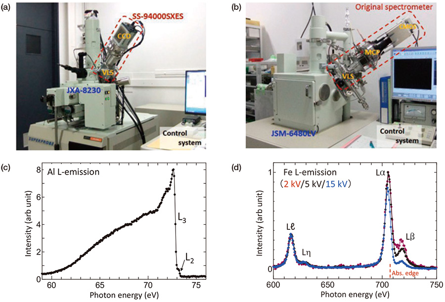
SXES instruments used in this report. (a) EPMA (JEOL JXA-8230) attached with a commercial SXES spectrometer system (SS-94000SXES) and (b) SEM (JEOL JSM-6480LV) attached with our original spectrometer. (c) Al L-emission spectrum obtained by (a). A fine structure due to a spin-orbit splitting of L3 and L2 levels of 0.4 eV is seen. (d) Fe L-emission spectra obtained by our original spectrometer (b) at accelerating voltages of 2, 5 and 10 kV. Spectrum intensities were normalized by Lℓ emission.
Metallization of Si sp3 network in Na8Si46
Figure 3(a) shows a crystal structure of Type-I Na-Si clathrate of Na8Si46. This material based on a three dimensional Si-sp3 covalent bonding network, which corresponds to a replacement of hydrogen bonds in gas hydrates by Si-Si covalent bonding. This Si-sp3 bonding network includes Si20 (dodecahedron) and Si24 (tetra-kaidecahedron) cages. Na atoms locate in those cages. Si-sp3 bonding network has a semiconductor character. However, Na atoms in the cages transfer it's valence electron to the Si network resulting in a metal character of Na8Si46 [12]. Figure 3(b) shows a SEM image of a bulk crystal used. Si L-emission spectrum obtained from a circled area in (b) by using the instrument of Fig. 2(a) is shown in (c). A Si L-emission spectrum of Si wafer (semiconductor) is also shown for comparison. Those intensity distributions are due to transitions from valence bands to inner Si-L2,3 levels with p symmetry. Due to a dipole selection rule, those intensity distributions reflect density of states of valence band with s and d symmetries. Labels L2’ and L1 written in the spectrum of Si wafer indicate special points in the band diagram of cubic Si crystal. This two peak structure seems to be common for the two materials. It may originate from Si-sp3 bonding network for the both materials. Contrary to this similarity, the right hand side end, where corresponds to the top of the valence band, is different each other. Na8Si46 shows a sharp peak. From a comparison with a theoretical calculation, this sharp peak may be assigned to a bonding state between Si cage and Na atoms [13]. For clarifying the difference more clearly, the spectrum of Na8Si46 is magnified in Fig. 3(d). At the right-hand side end of the spectrum, a sharp intensity drop with a width of 0.2-0.3 eV is seen as indicated by a vertical line. As the width is comparable to the energy resolution of the measurement, this sharp intensity change can be assigned to a Fermi edge structure, which apparently shows this material is a metal.
Fig. 3
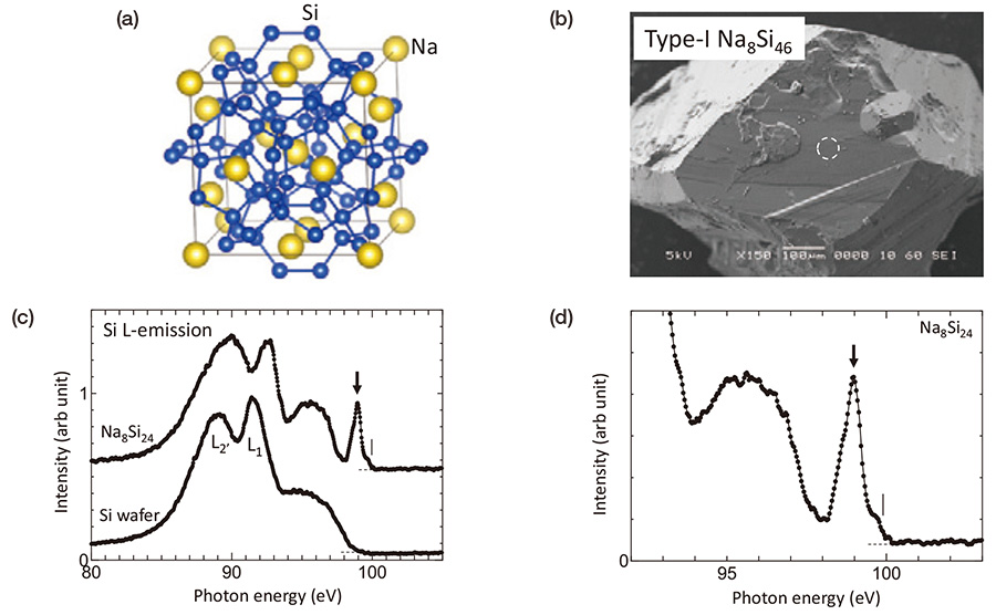
(a) Crystal structure of Type-I Na-Si clathrate of Na8Si46. (b) SEM image of a bulk crystal used. (c) Si L-emission spectrum obtained from a circled area in (b). (d) Magnified spectrum of Na8Si46 corresponds to the top of the valence bands. A sharp intensity drop with a width of 0.2-0.3 eV, indicated by a vertical line, corresponds to a Fermi edge structure.
Chemical state mapping of Na-doped CaB6
The crystal structure of CaB6 is composed of a network of B6 octagonal clusters, which locate at each corner of a cubic unit cell, and a metal atom at the body-center positon of the cell (Fig. 4(a)). Ca atom can transfer two valence electrons to the B6 cluster network. Since B6 cluster network can accept two electrons in valence bands, CaB6 becomes a semiconductor (n-type). For realizing a thermo-electric device using B6 cluster network materials [14], p-type semiconductor is necessary. As Na atom has only one valence electron, Na substitution to Ca site is a hole doping to B6 cluster network causing a p-type semiconductor [15]. From an EDS evaluation, Na content of the material was a few percent. However, the uniformity of the material has not been evaluated. Then, a piece of Na-doped CaB6 material was examined by using a commercial SXES-EPMA instrument of Fig. 2(a).
Figure 4(b) and (c) show a secondary electron (SE) image and a back-scattered electron (BSE) image of an area of Na-doped CaB6, respectively. The SE image shows a little different surface morphology in the upper left area, where the carbon signal was detected. The BSE image shows a lower intensity region in the center. Then, SXES mapping measurement was conducted. Spectral intensity maps of Ca-ℓ, η intensity (150-154 eV), B-K intensity (170-188 eV), and the top part of the B-K intensity (187-188 eV) are shown in Fig. 4(d), (e) and (f), respectively. Ca-ℓ, η emission map shows a low intensity for the dark area of the BSE image. It means a low Ca content for the area. B-K emission map does not show an apparent intensity change for the area. On the other hand, the map of the top part of the B-K emission intensity in Fig. 4(f) shows a larger intensity for the area. For investigating the origin of this intensity increase, B-K emissions spectra of the points of A and B shown in the figure are presented in Fig. 5. The spectra show a little difference in those intensity distributions, suggesting some difference of bonding state of B6-cluster network. It should be noticed that the peak of spectrum A indicated by an arrow locates in higher energy side by about 0.7 eV compared to that of spectrum B. This shift of the spectrum A should be a chemical shift originated from an energy shift of B 1s level to a larger binding energy side. This core-level shift can be due to a decrease of valence charge of B atoms. It is expected for Na-doped CaB6. Unfortunately, present system cannot detect Na-K emission intensity (coming up soon as a commercial version). Impurity oxygen can be also an origin because O atoms adopt electrons. Actually, a tiny intensity at 175 eV in the spectrum A can be assigned to the 3rd order intensity of O-K emission. In anyway, a high energy resolution soft X-ray mapping can give us a chemical shift mapping reflecting an amount of valence charge.
Fig. 4
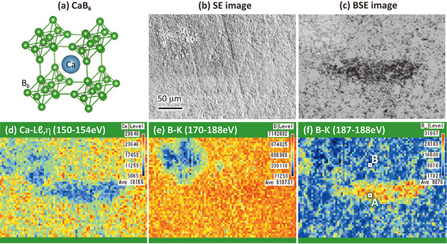
(a) Crystal structure of CaB6. (b) Secondary electron (SE) image and (c) back-scattered electron (BSE) image of Na-doped CaB6. Spectral intensity maps of (d) Ca-ℓ, η intensity (150-154 eV), (e) B-K intensity (170-188 eV), and (f) the top part of the B-K intensity (187-188 eV).
Fig. 5
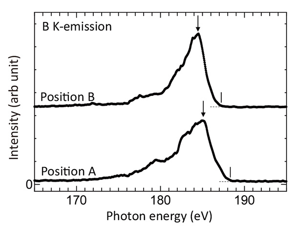
B-K emissions spectra of the points of A and B shown in Fig. 4(f).
Information on L-emission of 3d transition metal elements
Bonding state and valency of 3d transition metal (3d-TM) elements is a key for evaluating positive electrode materials of Li-ion battery, because a change of valency of 3d-TM elements is an origin of charge and discharge of the battery. Information on valence electrons of 4s and 3d of 3d -TM elements is included in L-emissions of the elements. As those energies of 1st order spectra are out of the energy range of the commercial SXES spectrometer, the original spectrometer (Fig. 2(b)) was applied to evaluate L-emission spectra of Ti and its oxides [16], and Fe and its oxides. There are four types of L-emissions of Lα, Lβ , Lℓ and Lη . Lα and Lβ emissions are due to transitions of valence electrons to inner L3-shell and L2-shell, respectively. Thus, those intensities include information on energy states of 3d electrons. On the other hand, Lℓ and Lη emissions are due to transitions from a shallow inner-shell level M1 to the deeper L3 and L2 levels, respectively. Thus, information included in Lℓ,η , is different from that of Lα,β. Figure 6 shows a schematic diagram of those transitions. Transitions from M2,3 to L2,3 are forbidden by dipole selection rule.
Figure 7 shows (a) L α,β emission and (b) Lℓ,η emission spectra of metal-Ti, a recently reported mono-oxideε-TiO and TiO2 (rutile). It is clearly seen that intensity distributions of L α,β emissions are different for different materials. Those reflect that energy states of bonding electrons are different for different atomic arrangements or crystal structures. In a simple ionic model, TiO2 is considered as Ti4+O-22 and cannot emit L α,β intensity because a Ti4+ ion has no 3d electron. Since L α,β emissions are observed in experiment, Ti atom in TiO2 is not a pure Ti4+ ion via covalent bonding between Ti and surrounding O atoms. For discussing intensity distributions of L α,β emissions, not only the density of state of valence bands but also energy shift of inner shell level (chemical shift) has to be considered. Furthermore, overlapping of Lα and Lβ intensity distributions and a presence of an absorption edge between Lα and Lβ has to be taken into account. On the other hand, intensity distribution of Lℓ,η due to transitions between two inner-shell levels is much easier to discuss.
Lα peak energy of TiO2 is about 2 eV smaller than that of metal-Ti. In turn, Lℓ peak energy of TiO2 is 0.7 eV larger than that of metal-Ti. L osition of ε-TiO is almost the same with that of metal-Ti. In case of Fe and its oxides shown in Fig. 7(c), Lℓ of metal-Fe and Fe3O4 is almost the same energy positon. L of Fe2O3 positons a little higher energy side of about 0.2 eV than others. Those suggest that the origin of the energy shifts of Lα and Lβ is not simple. A larger intensity ratio of Lβ /Lα in Fe oxides can be due to a suppression of Coster-Kronig process in oxides [18].
Based on a discussion on a binding energy shift due to a change of chemical effects in X-ray photoelectron spectroscopy, information included in Lα and Lℓ emission intensity is concluded as follows [16]. A change of Lα emission intensity distribution reflects changes of a valence charge and solid state effects (crystal-field, density of states, bandgap and etc.). A change of Lℓ peak position is caused by a change of a M1 core-hole effect in the final state, which reflects a local screening effect. WIEN2k code was used to evaluate a difference of core-hole effect in metal and its oxides. The values of TiO2 compared with metal-Ti and of Fe2O3 compared with metal-Fe were +0.7 eV and +0.2 eV, respectively. Those values well reproduce the experimentally observed values. This peak shifts due to core-hole effect are closely related to dielectric property, band-gap energy of a material examined [19, 20].
Fig. 6
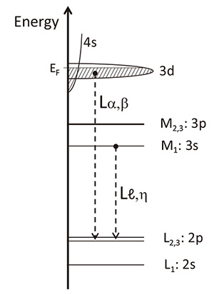
Schematic diagram of electronic transitions related to Lα,β and Lℓ,η emissions.
Fig. 7
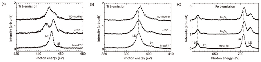
(a) Lα,β emission and (b) Lℓ,η emission spectra of metal-Ti, a recently reported ε-TiO and TiO2 (rutile). (c) Fe L-emission spectra of metal-Fe and its oxides.
Conclusion
Recently commercialized SXES instrument for EPMA and SEM has an energy resolution of 0.2 eV for Al-L-emission, which is about 10-100 times better than WDS and EDS. This SXES method is useful as a spectroscopy method for chemical state analyses and those mapping of bulk materials as TEM-EELS method for thin specimens. As there is no need for thin specimen preparation, this EPMA/SEM-SXES can make a quick feedback to material production processes. This instrument provides a bonding electron spectroscopy method not only for a wide variety of new functional materials developments but also for basic research of compounds.
Acknowledgments
The authors thank to Dr. H. Morito of Institute of Materials Research, Tohoku University for supplying a single crystal of Na-Si clathrate. SXES study on Na-doped CaB6 is a joint research with Prof. M. Takeda of Nagaoka University of Technology. Evaluation of chemical shifts of L-emissions of 3d transition metal elements by using WIEN2k code were a collaborated work with Dr. S. Koshiya and Dr. K. Kimoto of National Institute of Materials Science. Those works were partly supported by the Research Program of "Dynamic Alliance for Open Innovation Bridging Human, Environment and Materials" in "Network Joint Research Centre for Materials and Devices".
参考文献
- H. Takahashi, T. Murano, M. Takakura, N. Handa, M. Terauchi, M. Koike, T. Kawachi, T. Imazono, N. Hasegawa, M. Koeda, T. Nagano, H. Sasai, Y. Oue, Z. Yonezawa and S. Kuramoto, JEOL News , 49, 73 (2014).
- H. Takahashi, T. Murano, M. Takakura, S. Asahina, M.Terauchi, M. Koike, T. Imazono, M. Koeda and T. Nagano, IOP Conf. Series: Materials Science and Engineering , 109, 012017 (2016).
- Y. Sato, M. Terauchi and K. Adachi, Journal of Applied Physics , 112, 074308 (2012).
- O. L. Krivanek, T.C. Lovejoy, N. Dellby, T. Aoki, R. W. Carpenter, P. Rez, E. Soignard, J. Zhu, P. E. Batson, M. J. Lagos, R. F. Egerton and P. A. Crozier, Nature, 514, 209 (2014).
- M. Terauchi, chapter 7 in Transmission Electron Microscopy Characterization of Nanomaterials , ed. Kumar CSSR (Springer-Verlag), 287 (2014).
- M. Terauchi, H. Yamamoto and M. Tanaka, Journal of Electron Microscopy , 50, 101 (2001).
- M. Terauchi and M. Kawana, Ultramicroscopy , 106, 1069 (2006).
- M. Terauchi, H. Takahashi, M. Takakura and T. Murano, Handbook of Soft X-ray Emission Spectra ver. 3 (IMRAM Tohoku Univ. & JEOL), (2016).
- M. Terauchi, H. Takahashi, M. Takakura, T. Murano, M. Koike, T. Imazono, T. Nagano, H. Sasai and M. Koeda, Microscopy and Microanalysis , 22(Suppl 3), 414 (2016).
- S. J. B. Reed, Electron Microprobe Analysis 2nd edition (Cambridge Univ. Press.), 200 (1993).
- S. Ishii, M. Terauchi, Y. Sato, N. Tamura, M. Aono and H. Abe, submitted to Microscopy (2018).
- A. Moewes, E. Z. Kurumaev, J. S. Tse, M. Geshi, M. J. Ferguson, V. A. Trofimova and Y. M. Yarmoshenko, Phys. Rev. B, 65, 153106 (2002).
- Z. Wei, C. Quing-Yun, Z. Zhao-Yi and C. Ling-Cang, Chin. Phys. B , 24, 107101 (2015).
- M. Takeda, M. Terui, N. Takahashi and N. Ueda, J. Solid State Chemistry , 179, 2823 (2006).
- H. Kuribayashi, S. Makino and M. Takeda, Abstract of ISBB-18 , 148 (2014).
- M. Terauchi, S. Koshiya and K. Kimoto, IOP Conf. Series: Materials Science and Engineering, 304, 012018 (2017).
- S. Amano, D. Bogdanovski, H. Yamane, M. Terauchi and R. Dronskowski, Angewandte Chemie , 55, 1652 (2016).
- E. Antonides and G. A. Sawatzky, J. Phys. C: Solid State Phys ., 9, L547 (1976).
- K. Hirose, M. Kihara, H. Okamoto, S. Shinagawa, H. Nohira, E. Ikenaga, M. Higuchi, A. Teramoto, S. Sugawa, T. Ohmi and T. Hattori, Applied Physics Letters, 89, 154103 (2006).
- K. Hirose, H. Suzuki, H. Nohira, E. Ikenaga, D. Kobayashi and T. Hattori, J. Physics: Conference Series, 100, 01211 (2008).
Are you a medical professional or personnel engaged in medical care?
No
Please be reminded that these pages are not intended to provide the general public with information about the products.