Developing a New SEM with Seamless Surface Imaging to Elemental Analysis and Reporting
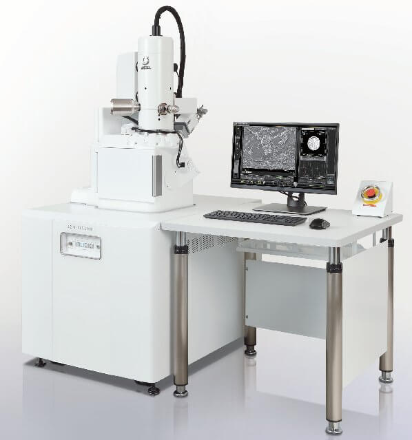
In August 2017, JEOL released its latest state-of-the-art scanning electron microscope (SEM), the JSM-IT500HR. The new JSM-IT500HR delivers the maximum practical magnification of x100,000 and also integrates an energy dispersive X-ray spectrometer (EDS) with the system. This next-generation SEM enables operations for various applications such as surface imaging, elemental analysis, and report creation to be performed seamlessly. In the following behind-the-scenes development of the SEM, we introduce to you our development team members whose “non-stop” drive and passion have made the launch of JSM-IT500HR possible.
Yusuke Ishida
Development Team 2, Development Group, Development Dept.,
JEOL Technics Ltd.
Ryouta Mishima
Development Team 1, Development Group, Development Dept.,
JEOL Technics Ltd.
Hirofumi Kuwahara
System Group 2, System Development Dept.,
JEOL Technics Ltd.
Hisashi Zaimoku
System Group 2, System Development Dept.,
JEOL Technics Ltd.
Developing a New SEM with Seamless Surface Imaging to Elemental Analysis and Reporting
JEOL Technics: in Pursuit of the Ultimate SEM
JEOL Technics Ltd. is a developer and manufacturer of high-performance and multi-purpose SEMs. SEMs are electron microscopes used for imaging the surface of specimens. A focused electron beam is used as a probe to trace the surface of the specimen. Due to interaction with the beam, the specimen emits signals of varying intensity called “secondary electrons” or “backscattered electrons,” which are detected by the SEM to produce an image that discloses the topographic and compositional information on the surface of the specimen.
JEOL Technics’s SEMs are capable of imaging a wide range of biological, organic, and inorganic specimens.
SEMs are not limited to just laboratories. They are widely used for quality control and safety inspection in industries such as manufacturing of home appliances, automobiles, and food. Hence, SEMs are used by a diverse group of users who require that their SEMs intuitive and user-friendly so as to enable them to operate the SEM with ease and without the need to consult an instruction manual. This was the challenge that the SEM development team faced when they first set out to design the next generation of SEMs.
Challenge of Reduced Development Time
In September 2014, in response to user demand and market trends, JEOL Technics Techniques established a team of engineers and developers who were assigned to design and construct a new multi-purpose SEM that would accommodate all types of users. The new SEM would give users the ability to view specimens at a very high magnification and would include a built-in capability to integrate an EDS for seamless elemental analysis. The development team faced two major technical challenges: The first was to realize the ability to obtain a clear image of the target site at any magnification. The second was to integrate the EDS, a critical function of elemental analysis, with the SEM system to streamline analysis. This latter issue was critical because of the high usage of the elemental analysis feature. In fact, 80% of users report using the SEM for elemental analysis on micro-areas submicron structures and foreign materials as well as for surface imaging. The EDS system is generally purchased separately from an EDS manufacturer and is then attached to the SEM instrument as an external attachment. However, since JEOL is the only manufacturer that produces both SEM and EDS systems, the idea of integrating observation modes and analysis functions seemed like a natural outgrowth of the company.
Perhaps, the greatest challenge to the team was the deadline for completion. They had two years. President of JEOL Technics stressed the urgency: “We need to promptly satisfy the diversified needs and the fast-changing market.”
Although his team members thought this target was impossible, Yusuke Ishida, the team leader, understood and recognized the urgency. For years Ishida directly worked with customers as an instrument maintenance and service representative and would often get feedback about the need to improve the SEM. He viewed this project as a good opportunity for the company.
Ishida and his team members started work on the project. They considered the specifications for the SEM and methods for development for the same.
Although the team agreed on improving the usability of the SEM instrument, each person had different concerns given their different roles. For example, one said “Among all, the magnification should be sufficiently high.” While another argued “It would be better to improve the user interface first.” During their discussions, Ishida would keep an open mind while staying focused on usability goals and workable specifications.
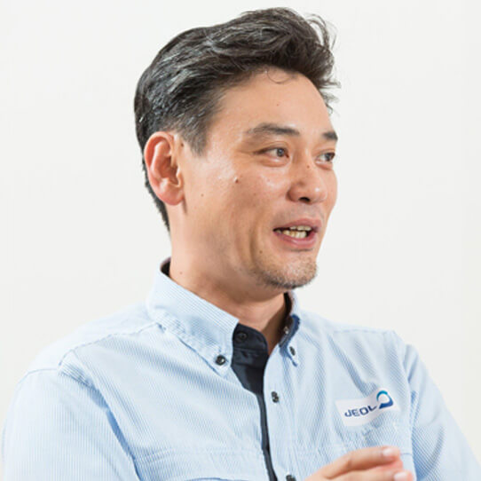
Yusuke Ishida
Development Team 2, Development Group, Development Dept., JEOL Technics Ltd.
Hobbies & Skills :Eating tour, Boston Red Sox fan
Given his service-engineer experiences with domestic and overseas customers, Ishida led the team and brought to the development project his knowledge of what users want.
Automatic Transmission Supercar
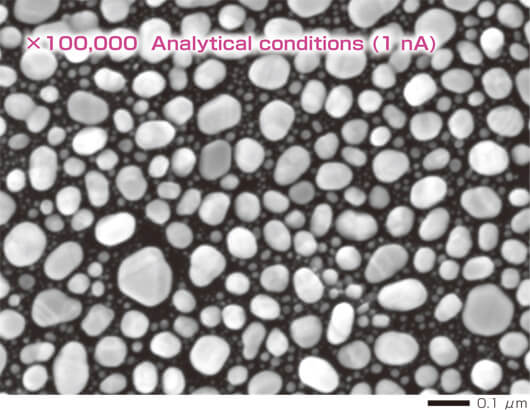
Specimen : Au particles
Accelerating voltage : 15 kV, Magnification ×100,000
High-vacuum mode, Secondary electron image
The development team started working to improve the maximum practical magnification. Conventional multi-purpose SEMs have the magnification of x20,000. This magnification is not enough to observe minute foreign substances or defects at or below 0.1 μm and is a requirement of precision instrument applications. For these applications, a magnification of x100,000 is required. Use of high-quality, high-brightness electron guns has been considered because they deliver a narrower electron beam than that delivered by conventional tungsten (W) or lanthanum boride (LaB6) electron guns and would substantially boost magnification. However, to improve magnification, the electron gun chamber must be located in an ultra-high-vacuum state with barely any gas molecules. These types of electron guns are expensive and are used in high-end SEM models that are manufactured for lab-quality performance and thus require delicate handling. The market demanded was an affordable, simple-to-use, multi-purpose, specimen-compatible SEM with x100,000 magnification.
To keep the instrument affordable, the team opted to fit the gun into a compact enclosure and configured it for easy handling.
Ryouta Mishima, another development team member and expert in designing the electron optical system, shared an important insight: “I wondered both users and developers get caught too much in the common sense that 'SEM is difficult.”
In reality, he argued that SEM users want images and data for their analysis. They are not that interested in making full use of the system. If that is true, then there must be ways to minimize manual operations even though that may not yield the highest quality performance. Handling delicate optical systems can be rendered easy and straightforward with more advanced control technologies and schemas. “An automatic adjustment button can solve all the issues. We could make automatic transmission supercars but we had created only manual transmission supercars” said Mishima.
While the project showed good progress, the team encountered an unexpected problem during the last six months of development. The power supply for the SEM, which was a high voltage tank, needed to be replaced. There were two tanks at that time but the development team was divided as to which tank to choose. The methods to control each of the tanks were different. The electric circuit and hardware for either tank required substantial reworking. With only six months left before the release date, the designers did not have enough time to design the control circuit if they had to wait for a final decision about the tank. Everyone was at loss about what to do next. Hirofumi Kuwahara, a quiet man in charge of firmware development, spoke up: "So, there would be no problem if I make firmware that works in both scenarios.” With those words, Kuwahara set out to do just that. He completed the firmware to accommodate either tank in less than six months. Kuwahara’s spirited work made possible by his strong will to meet the product release timeline led to the completion of the SEM hardware by the two-year anniversary of the project kick-off.
Ryouta Mishima
Development Team 1, Development Group, Development Dept., JEOL Technics Ltd.
Hobbies & Skills :Workout (career: 1.5 months)
In charge of design and development, which are decisive factors in SEM performance. In this development project, Mishima improved the efficiency of the optical column of the multi-purpose SEM and successfully brought a low-cost integration of a high-brightness electron gun into reality.

Hirofumi Kuwahara
System Group 2, System Development Dept., JEOL Technics Ltd.
Hobbies & Skills :Jogging, Home gardening
In charge of firmware development. In this development project, he completed the firmware within the time limit with a strong sense of responsibility and processional moral despite unexpected and sudden change of the entire electric circuit for the high-voltage tank.