The Challenge of Manipulating Light-Electron Beam Lithography System Draws the Future
INTERVIEW 05
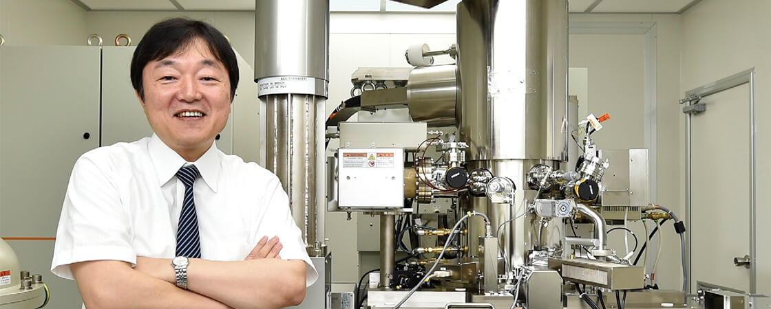
Professor Susumu Noda
Graduate School of Engineering and Faculty of Engineering, Kyoto University
Optical chips, semiconductor laser innovations, thermal emission control and high-efficiency solar cells, etc… Photonic crystals are without doubt innovative materials that catch the future. Professor Susumu Noda of Kyoto University has led studies in this field since the very beginning and continues to run toward an ambitious dream.
Ultra-modern Material – Photonic Crystals
With the capacity to split, bend, store and reinforce light, “photonic crystals” are innovative materials that possess great potential to manipulate light freely and thereby bring about a great leap of possibilities for electrical and electronic devices. As light has the advantages that it travels much faster than electrons and hardly attenuates even when traveling long distances, there have been diverse attempts to marry it with electronics. However, while flows of electrons can be manipulated freely with semiconductors, for light, no such equivalent semiconductors existed. Photonic crystals virtually serve as “semiconductors for light” that allow for the manipulation of light, as can be done for electrons.
One example of possible applications of photonic crystals is an optic-wired computer with internal substrates made with photonic crystals. For conventional substrates, data are transmitted by electrons between components such as CPU and memory. However, the velocity of electrons is limited and electrons necessarily generate heat, which has been one of the major factors that prevent an improvement in computer processing speed. Utilizing substrates made with photonic crystals, however, data can be carried by light between components. Technologies to store intense light at one point by using photonic crystals have already been invented. Advancing such technologies will ultimately realize today’s supercomputer performance in a consumer-size computer.
Photonic crystals are also expected to trigger a revolution in semiconductor lasers. While semiconductor laser technology has been significantly advanced in terms of wavelength and time, it is left behind other laser technologies including solid-state lasers and gas lasers in terms of power. Additionally, its advancement in power has been long overdue. If large-area coherent operations are fully realized by photonic crystal lasers, it is expected that high-power operations with consistently high beam quality will be possible, which will cause a new revolution in the field of semiconductor lasers. Possible applications thereof range from processing, automotive and sensing industries to ignition lasers for nuclear fusion. Its potential market size is remarkably large.
Photonic crystals are also expected to trigger renovation of thermal emission technologies. Thermal emission herein refers to the phenomenon of light (electromagnetic wave) generation from a heated object. For many years, this phenomenon has been utilized as an underlying principle of lamps and light sources for analyses. In this sense, the sun is also a thermal emitter, radiating light in an extremely broad band from ultraviolet light to infrared light. Similarly, general thermal emitters radiate a broad range of light not needed for specific purposes and this greatly degrades light use efficiency. What if thermal emission from objects can be converged into desired wavelengths and desired linewidths with no energy loss and be controlled dynamically and at ultra-high rates? It will realize high-efficiency and high-rate infrared light sources for various analysis purposes and significantly improve efficiency of thermophotovoltaic power generation system.
Structure to Manipulate Light Freely
Light has wave-like characteristics, and differences of wavelength in the visual light range are represented as different colors. The reason why sunlight and fluorescent light look white to us is due to synthesis of light in various wavelengths. A red post looks red because the light reflected from the post is red and the other light is absorbed or transmissive. Reflection, absorption and transmission of light are determined by an object’s molecular and surface structures. Photonic crystals are meant to design and produce such micro structures to freely control light reflection (i.e. changing light direction) and light resonance (i.e. reinforcing light).
The procedure to make the photonic crystals is simple. As in the case of semiconductors, the primary material component is a silicon wafer (or an III-V compound semiconductor wafer). The procedure is as follows: First, use an electron beam to create orderly-aligned air-holes on a wafer. This brings air into the pores. Then a large number of recurrent patterns with different refraction indexes are created in between semiconductor parts and reflection occurs at the boundaries. Consequently, it causes a Bragg reflection phenomenon in which light reflected from boundaries in a specific direction interferes constructively and other light interferes destructively and disappears, and results in a so-called “light insulator.”
Structures called “artificial defects” are more important. When air-holes of different sizes or shapes and/or sections with no air-holes are created on the pattern of orderly-aligned pores, the presence of light is allowed in such sections, making it possible to transmit or store light through the sections. These “defects” serve as cages of light. Therefore, it is possible to flexibly control how light propagates by arranging the defects accordingly. (Fig.1 illustrates a three-dimensional view of an example photonic circuit on a photonic crystal wafer.) Also, if micro defects (including micro-variations of defect sizes) are made, light will converge into the defects and only light of wavelength(s) appropriate to the air-holes size will interfere constructively. Such structures will realize light-storing memories for photonic circuits and micro laser devices. (Fig.2 shows a two-dimensional electron micrograph of optical waveguide and nano-resonator formed on a photonic crystal wafer.) Nonetheless, the air-hole diameter is as fine as approximately 200 nm, which is even smaller than the size of a virus, and this means accuracy by nm is required for manufacturing. To achieve desired functions, air-hole locations must be controlled in sub-nanometers and a highly precise machine is required.
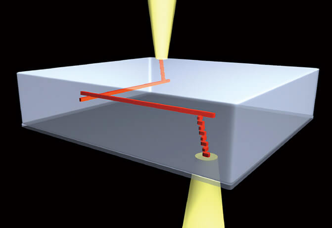
Fig.1
Three-dimensional image of a light path through a photonic crystal
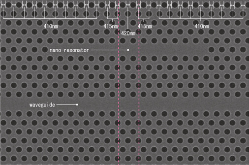
Fig.2
A two-dimensional pattern of orderly-aligned air-holes with “artificial defects” applied. The portion indicated as “Nano-resonator” (between the dashed lines with 10 mm wider pore intervals) can confine light longer. The portion indicated as “Waveguide” (its height is larger than that of the nano-resonator) serves to guide light from outside to the nano-resonator. As pore diameter and intervals should be controlled in nanometers, precision drawing by an electron beam lithography system is required.
A Prime Figure behind Practical Applications of Photonic Crystals
Currently, Professor Noda’s laboratory uses JEOL state-of-the-art electron beam lithography system to draw the path to the future.
Susumu Noda, a Professor at Kyoto University, has been actively engaged in development of photonic crystals since the 1980’s.
After completing graduate school, young Professor Noda joined the Central Laboratory at Mitsubishi Electric Corporation and continued research on laser technologies. Reaching a certain point of satisfaction in his research, he began exploring possibilities of next-generation optical materials and focused his attention on photonic crystals. Coincidentally, his former professor offered him an assistant position at Kyoto University and he decided to return to academia for basic research.
“At that time, Japan was at the zenith of its bubble economy. As such, the research environment of private enterprises was far better than that of academia because university laboratories could, at best, only obtain several millions of yens per year for research expenses. They were so poor that some used empty sake bottles as beakers,” he reflected.
The professor said photonic crystals represented such a big dream that it made him enthusiastic about continuing the study in such difficult conditions.
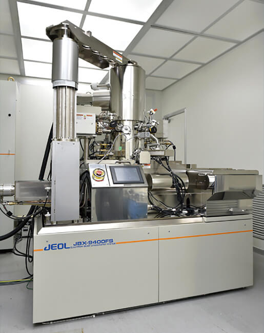
“When I started the research, many researchers questioned its practical possibility and they believed it to be a mere fantasy. Even so, I still believed photonic crystals would realize key devices for the future if put into practice."
Due to the shortage of funds and immature nano-engineering technologies, his research could not go beyond the theoretical phase. A large part of the leap in his photonic crystal research was a result of the progressive development of devices called electron beam lithography systems. We can call this machine (photo on right) “nano-printer” as it draws design data developed by CAD, etc. on nano-materials by using an electron gun that emits electrons in the form of beams. This technology has been used as an electron-emitting source of electron microscopy. JEOL went into the business of electron beam lithography systems in 1967 with its long-standing technologies and experiences in electron microscopy business and improved the system’s performance step by step in accordance with the voices of researchers.
“JEOL’s lithography system accurately locates the object and draws with great precision. The acceleration of our research is surely attributable to the improvement of such systems.”
The Pursuit of Future Standard Devi
The Pursuit of Future Standard Devices
After consistently dedicating himself to low-profile basic research for over 10 years, a paper he published in 2000 catapulted Professor Noda into the limelight. The article demonstrated the feasibility of photonic crystal technology with the abundant fruits of his long-standing research, which were substantial enough to involve a multitude of researchers. Today, there are a number of applied researches of photonic crystals aiming to generate tangible outcomes.
One of the most expected applications of the technology is the aforementioned large-area coherent semiconductor laser. As of this writing, watt-class operations of high-quality and high-power beam output with a single chip have been successfully carried out. Researchers expect that the world will change when 10W operations are put into practice. Also, an application in solar cells has attracted attention as a renewable energy source. Existing solar cells can absorb and convert only a part of visible light into power so a large part of sunlight is abandoned. The themal emission control with photonic crystals (mentioned earlier), is expected to solve the issue in the future; i.e. thermal emission control could improve power generation efficiency by allowing for solar cell designs that emit light in a specific band for the most efficient absorption by the cells and allow them to absorb most of the sunlight.
Admiring his achievements that opened up the possibilities of such novel technologies, many researchers believe Professor Noda deserves the next Nobel Prize.
"Practical use of photonic crystals is just getting started. My mission is to steadily nurture the budding technologies to their full bloom,” he said.
Susumu Noda
Professor of Graduate School of Engineering and Faculty of Engineering, Kyoto University
After finishing the master’s course in the Graduate School of Engineering and Faculty of Engineering, Kyoto University, Professor Noda joined Mitsubishi Electric Corporation. In 1988, he assumed the post of an assistant in the Faculty of Engineering, Kyoto University, an associate professor in 1992 and a professor in 2000. In the same year as becoming a professor, he was awarded the 14th IBM Japan Science Prize for Research on Semiconductor Photonic Crystals and Applications. Subsequently, Professor Noda received a series of awards including the Commendation for Science and Technology by the Minister of Education, Culture, Sports, Science and Technology in 2009, the 6th Reona Ezaki Award in 2009, the Medal with Purple Ribbon in 2014 and JSAP Outstanding Achievement Award in 2015, etc.
Posted:May 2016