A Synchrotron on your Desk? Seeing everything with an electron microscope
INTERVIEW 02
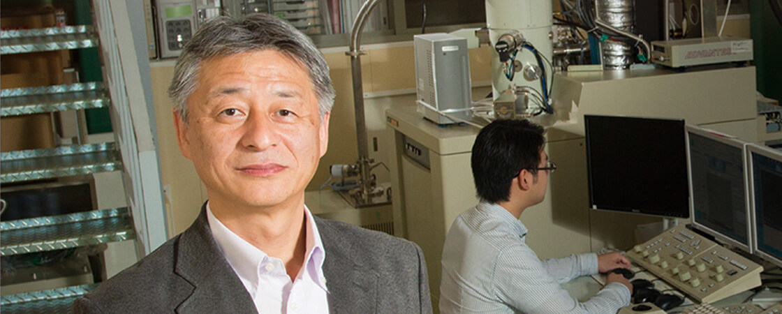
Professor Masami Terauchi
Institute of Multidisciplinary Research for Advanced Materials (IMRAM),
Tohoku University Laboratory of Electron Crystallography and Spectroscopy
What is this thing in front of us? To make an accurate identification, we must know the chemical bonding state. What if we could see everything with the electron microscope?
The development of an instrument that started with the idea of one microscopist is causing a revolution in manufacturing.
Tabletop Synchrotron Facilities?
“It’s almost like having a synchrotron on my desk”
Professor Masami Terauchi of Institute of Multidisciplinary Research for Advanced Materials (IMRAM), Tohoku University, smiles as he comments.
A synchrotron is a facility that produces beams over a wide range of energies, from soft X-ray to hard X-ray and infrared light. It is used to measure arrangement of elements and chemical bonding states (electronic states) of specimens. SPring-8 is a high-power synchrotron facility in Hyogo prefecture. The storage ring alone has a diameter of more than 450 meters. It is an enormous facility that completely surrounds an entire hill.
The major observations that could only be made with a facility of this size are now possible with a machine that fits on top of a desk. This ground-breaking achievement was the result of a project of Collaborative Development of Innovative Seeds (Practicability verification stage), Japan Science and Technology Agency (JST), involving JEOL, Tohoku University, Shimadzu Corp., and Japan Atomic Energy Agency (JAEA) working to develop a “High-energy resolution soft X-ray spectrometer for use with an electron microscope”. The combination with the electron microscope results in an instrument that reveals the chemical bonding state of materials.
Soft X-ray spectrometer mounted on tungsten SEM. Routinely used in the lab.
3 factors that determine material’s characteristics
When developing new materials, there is naturally a need to figure out what kind of thing has just been created. To answer the question “what is it?” there are three attributes that must be characterized; crystal structure, chemical composition, and chemical bonding state. The crystal structure can be readily observed at the sub-nano level with transmission electron microscopes (TEM) and scanning transmission electron microscopes (STEM), for which the resolution has been rapidly increasing in recent years. For the composition, meaning the elements that are present in the material, not only is it possible to perform qualitative and quantitative analyses with X-ray emission spectroscopy (XES), but this can also be combined with an electron microscope to capture images of the distribution of the elements.
For the final attribute, the chemical bonding state is determined by the energy state of electrons. For example, even things made from the same element can have very different properties, such as charcoal, diamond, fullerene, or graphene, which are all composed of carbon (C) atoms. The differences in the properties arise from the differences in bonding states, the density of the electrons in any given orbit around the nucleus of the carbon atoms. To be able to see the energy state of electrons finally makes it possible to understand and identify the materials. Viewing the electrons and the bonding states has conventionally been the specialty of synchrotron facilities.
Seeing the chemical bonding states with an electron microscope
Professor Terauchi has been involved in the development of electron microscopes for a long time; but, one day he began to feel that something was still missing.
“With the advances in electron microscopes, it has become easy to see crystal structures, but it still was not possible to obtain a complete set of data without also applying an X-ray spectrometer and making use of a synchrotron. I began to wonder if it would be possible to obtain these three types of data using only the electron microscope.”
With this idea, the professor started his own research and development.
The electrons in the outermost orbital shell of atoms are closely associated with the chemical bonding. These are called the valence electrons. Accordingly, measuring the energy distribution of the valence electrons is very important for identifying the physical properties.
Photoelectron Spectroscopy (PES) is often used to observe the energy states of valence electrons. The technique of measuring the photoelectrons that are emitted from the sample surface when it is irradiated with a beam (ultraviolet or X-ray) has excellent accuracy; but, it is necessary to ensure that the surface of the sample is extremely clean, and to make the measurements under an ultra-high vacuum.
Another known approach is to use XES for composition analysis. Ultra-high vacuum is not required for the measurements, and there is no difficulty with insulating materials. Seeing the potential in this simplicity, Professor Terauchi made a series of prototypes of high-resolution XES devices that could be mounted onto an electron microscope.
When a beam is applied to a specimen, inner-shell electrons jump up over the valence bands (bonding states) and followed by transitions of valence electrons (bonding electrons) to the vacant inner-shell, emitting X-rays at that time. To capture this, if the energy and its intensity are measured, it is possible to determine the energy states of bonding electrons in the outermost shell. However, the energy spread of valence electrons is only about 5 to 10 eV, so an energy resolution of at least 1 eV is required.
“At the time the study was started in 2000, the concept was announced at an academic meeting. I still remember hearing people say that such a high resolution was impossible,” recalls Professor Terauchi.
Nevertheless, he continued his work.
There were 3 key components: a collecting mirror, a diffraction grating, and a detector.
In order to efficiently collect the X-rays that were scattered about, he designed his own mirrors. To compensate for image aberrations, a unique diffraction grating with systematically varied groove spacing was used. Furthermore, to catch weak soft X-ray signal, he obtained a special back-illumination CCD, with no anti-reflection coating. Working with these, he continued to make refinements.
JEOL joined the team in 2006, and the development to make a commercial version was started. Through this process, a specification was developed to enable detection of even lithium, which has a very low energy.
Overwhelming simplicity changes manufacturing
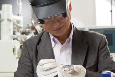
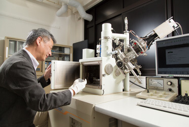
“Even with my aged eyes, it’s easy” Professor Terauchi said, wearing a headband magnifier, quickly setting a sample.
Thus, it was first combined with TEM. For the observation of the aluminum Al-L spectra, a soft X-ray spectrometer capable of measurements with a high energy resolution of 0.2 eV was developed. In 2013, the type that could be mounted to an electron probe microanalyzer (EPMA) or a scanning electron microscope (SEM) was announced. The detection sensitivity was 2 orders of magnitude better than conventional EPMA for boron, a useful additive for improving steel quality. Resolution was also improved by more than an order of magnitude compared to the conventional EPMA.
“Many of the elements that are key to the development of new materials, such as lithium, magnesium, boron, nitrogen, and carbon, emit soft X-ray signals when an electron beam is applied. This can now be observed in the field, at the site where the material development is being performed. We can expect to see an acceleration in the development of new, high value-added materials.“
“The main point is that this is a microscope. You can see the specimen and check the crystal structure. You can zoom in on an area of interest and analyze the chemical bonding state. This is not something that can be done at a synchrotron facility.”
The ability to acquire the data with SEM operations is also highly appreciated.
“As special sample preparation technique is not required, you can pick up a sample with a pair of tweezers, then you can set the specimen in about three minutes, then get data in five minutes. There is no doubt that this ease of use will cause big changes at production sites.”
Currently, JEOL offers the type fitted with EBSD (electron backscatter diffraction) for orientation analysis. With this system, it is possible to acquire the 3 types of data for “crystal structure”, “chemical composition”, and “chemical bonding state” all at once using a SEM. We are currently working hard to create the database for fingerprint check with spectra measured.
The time for entering into new paradigm for manufacturing is coming soon.
Application to new material for fuel cells
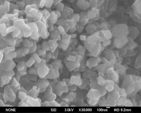
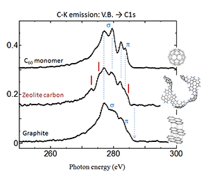
Zeolite template carbon (ZTC), a candidate material for fuel cell and electrode of rechargeable batteries, being researched by Prof. Kyotani at IMRAM, Tohoku University, has ball-like network structure without forming complete ball shape like C60. Soft X-ray spectrometry reveals that it is partially diamond-like, and partially curved graphene (C60) like. The existence of a special bonding state that is neither random nor periodic was confirmed with the high-energy resolution soft X-ray spectrometer.
Masami Terauchi
Professor, Institute of Multidisciplinary Research for Advanced Materials (IMRAM), Tohoku University
Ph.D. in Physics, Tohoku University, and also completed post-doctoral studies. Became an assistant in the Research Institute for Scientific Measurements , Tohoku University in 1990, later advancing to positions as lecturer, and assistant professor before accepting his current post in 2002. Received the Prize of the Crystallographic Society of Japan in 1995 for “Developments and Applications of CBED Method and its Extension to (3+1)-Dimensional Crystallography”, as well as the Prize of the Electron Microscopy Society of Japan (Setou Prize) for “Development of High Energy-Resolution EELS Microscope and Applications to Materials” in 2000. Also received Macres Award from the Microbeam Analysis Society in 2004 for “A High Energy-resolution Wavelength-dispersive Soft-X-ray Spectrometer for a Transmission Electron Microscope to Investigate Valence Electrons”.
Posted: January 2015