Super High Resolution Electron Microscopes Stimulate Progress in Materials Science
INTERVIEW 01
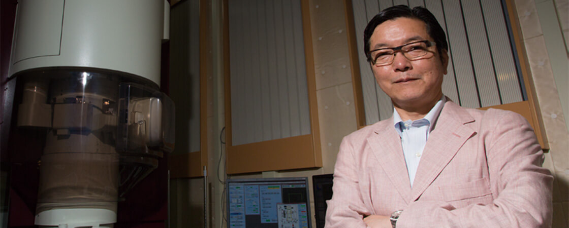
Professor Yuichi Ikuhara
Institute of Engineering Innovation, School of Engineering, the University of Tokyo
Shifting from production based on experience and intuition to rational manufacturing based on theory and evidence.
JEOL Super High Resolution Electron Microscopes support great strides in materials science.
Exploring grain boundaries
Industrial materials like metals and ceramics have a polycrystalline structure consisting of many tiny crystallite grains. The interface between crystallites is called a grain boundary. Grain boundaries play a role in determining the properties of the material, and have become an area of great interest in recent years.
“Non-periodic structure , such as the crystal surface, interfaces, dislocations, and atomic vacancies, have their own specific electronic structure. These are sources of functions that are not found in perfect crystals. If we can clarify the atomic and electronic structure of the grain boundaries as well as the mechanisms of the functions, this will have a significant impact on industry, contributing to the development of materials with new functions.”
So says Professor Yuichi Ikuhara of Institute of Engineering Innovation, School of Engineering, the University of Tokyo. He has been working on grain boundaries at atomic level since he was a graduate student, and continues his research with a heavy emphasis on observations and measurements using electron microscopes.
Paradigm shift in materials engineering
The advent of spherical aberration correction for scanning transmission electron microscopes (STEM) was a major breakthrough in this area of research. Due to the nature of round electron lens, there is an unavoidable blurring (spherical aberration) from the electron lens. However, by utilizing non-axial-symmetric magnetic fields generated by multipole lens, it is possible to largely eliminate this blurring, enabling direct, super-high resolution observation of objects at the Angstrom level. The theory behind this method has been known for some time, but practical implementation has been difficult. Since the late 90’s, the technologies to achieve this have been realized, and welcomed with delight by the research community.
Professor Ikuhara was one of those researchers.
“Figuring out why a material has a certain functionality can now be explained at the atomic level. This is probably one of the most significant paradigm shifts in the history of materials science.”
For example, it was known that adding small amounts of the rare earth yttrium to alumina (aluminum oxide) greatly increases the strength, but it was never fully explained why this occurs. Professor Ikuhara introduced one of the first Japan made commercial STEM systems incorporating spherical aberration correction. Using this instrument, he observed and compared the alumina interfaces both before and after the addition of yttrium. In this way, he confirmed that the yttrium atoms are located periodically at specific sites of the alumina grain boundaries, and that the alumina ionic bonds were changed to covalent bonds. This discovery was published in the journal Science in 2006. Since then, the power of spherical aberration correction has been harnessed for a range as a steady succession of discoveries.
Professor Ikuhara continued to announce important results of his analyses of grain boundaries at the atomic level, mainly through publications in journals like Nature and Science. In 2010, his achievements were recognized as the Humboldt Research Award (Germany); in 2013 he was awarded a Commendation for Science and Technology from the Minister of Education, Culture, Sports, Science and Technology.
In recent years, research has been progressing on the defect structures and dislocations that form ceramic crystal interfaces. Super-computers are used to perform the theoretical calculations to design ceramics with defect structures that are not found in existing materials. By observing these defect structures using the STEM with spherical aberration correction, it is possible to confirm whether the structures match the theoretical predictions.
Professor Ikuhara’s eyes sparkle as he remarks, “This is exactly opposite to the traditional approach of developing materials based on intuition and trial and error. The rational methods through calculation and observation to artificially control the structure of lattice defects will certainly accelerate future advances in materials science.”
Ultra high resolution observation of hydrogen atoms
Professor Ikuhara’s lab includes the world’s first ultra-high resolution electron microscope GRAND ARM manufactured by JEOL. Equipped with a cold cathode field emission electron gun in the standard configuration, with a maximum accelerating voltage of 300 kV and incorporating the latest version of JEOL’s own spherical aberration correctors, GRAND ARM is capable of STEM resolution of 45 pm※.
Professor Ikuhara voices his approval.
“Even light elements like hydrogen and lithium can be observed in detail, even when they are in close proximity. We can perhaps even say that the resolution is now sufficient.”
![HAADF-STEM image (left) and ABF-STEM image (right) of titanium oxide crystal with [110] orientation (Obtained with GRAND ARM).](/assets/img/products/technology_cases/interviews/01/img_interview_01_02.jpg)
HAADF-STEM image (left) and ABF-STEM image (right) of titanium oxide crystal with [110] orientation (Obtained with GRAND ARM).
It is possible to observe separately the adjacent oxygen atom columns in the ABF-STEM image
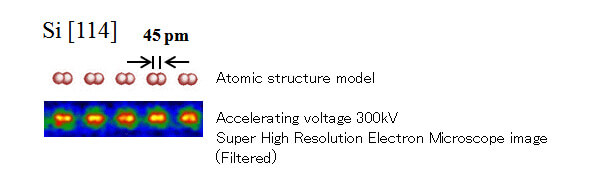
Atomic structure of silicon
He is also appreciative of the usability of the human interface and the large specimen tilt angle. “There are a number of engineers in the electron microscope group at JEOL who have studied materials science. Developing the instruments from the user perspective is what gives rise to the excellent usability.”
JEOL guaranteed value: 63pm
Innovation through Industry-Academia Collaboration
Behind this advancement is a more-efficient research and development system achieved through collaboration between industry and academia.
Since 2005, The University of Tokyo and JEOL have been operating a Business-Academia Cooperation Office. There are more than ten JEOL electron microscopes, including the GRAND ARM, installed at University of Tokyo facilities, supporting the research of Institute of Engineering Innovation, School of Engineering, the University of Tokyo. Feedback from the materials scientists who use these instruments is quickly incorporated into product design, contributing to the rapid evolution over the past several years.
“There are many visitors from abroad coming to see in the Business-Academia Cooperation Office GRAND ARM, focusing a lot of attention on its impact. Disseminating the observation methods and obtained results throughout the world may even lead to dramatic changes in every area of manufacturing.”
There are still more advances ahead in the evolution of STEM.
Yuichi Ikuhara
Professor, Institute of Engineering Innovation, School of Engineering, The University of Tokyo
Director, Nano-Engineering Research Center
Graduate of Kyushu University. After working in Japan Fine Ceramics Center and Case Western Reserve University (USA), joined the University of Tokyo as an associate professor in 1996. Assumed his current position in 2003. In 2010 received the Humboldt Research Award (Germany) for his work on the physical properties and hyperfine structures of material interfaces. Concurrently serves as a professor at the Advanced Institute for Materials Research, Tohoku University, and as Principal Researcher at the Nanostructures Research Laboratory of the Japan Fine Ceramics Center. American Ceramic Society Fellow and a member of the World Academy of Ceramics.
Posted:October 2014