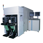
【DISCONTINUED】JWS-3000 Wafer Process Inspection System
DISCONTINUED
This product is no longer available.
If you would like to know the latest information about your preferred product or to find out more about alternatives, please click on the link below. We hope you will continue to use our products.
To improve the yield in the semiconductor manufacture process, the causes of defect must be examined by both visual observation and elements analysis in SEM.
Features
To improve the yield in the semiconductor manufacture process, the causes of defect must be examined by both visual observation and elements analysis in SEM.
JWS-3000 can link coordinate data, move the stage to the defect position easily, and then inspect & observe it on high resolution SEM by using online networking to various kinds of optical defect inspection systems. Using ADR (Auto Defect Review) and ADC (Auto Defect classification), The JWS can collect defect data automatically and classify to find the source quickly. An important feature is ease of operation without special training.
By employing a super-conical objective lens, the wafer can be tilted up to 45° without changing working distance. High resolution is maintained even in tilting observation.
It is not necessary to adjust each axis with changing observation conditions. The JWS can be equipped with various optional functions such as; CD measurement, optical microscope, EDS, INDEXER etc.
Accelerating voltage: 0 ~ 15kV
Resolution: 3nm at 1 kV
Long term Beam Stability by TFE Electron Beam (flashing unnecessary )
High resolution image at 45° Tilt of 300mm wafer by employing super-conical objective lens
User Friendly operation with advanced GUI
High throughput defect inspection on-line with communication to optical defect inspection systems
Low energy observation 100-500V for low-K material
High throughput in Automatic Defect Review mode
Auto Defect Analysis
Remote operation available
Superior VC & HAR imaging
Example of pattern defect observation by JWS-3000
The JWS-3000 can obtain useful information for improving yield in manufacture process. The source of the defect and particles can be observed at high magnifications as well as multiple changing of tilt and rotation angles.
Specifications
| Resolution | 3 nm (at 1kV), 5 nm (at 300 V) |
|---|---|
| Acceleration Voltage | 100 V to 20 kV |
| Observation Magnification | x 100 to x 500,000 |
| Stage | X-Y: 300 mm, T: 45°, R: 360° |
| Sample Size | 300 mm (for 200 mm is also possible) |
| ADR(die to die) | 750dph(JEOL standard sample) |
More Info
Are you a medical professional or personnel engaged in medical care?
No
Please be reminded that these pages are not intended to provide the general public with information about the products.