JEM-Z200MF
Magnetic field-free electron microscope
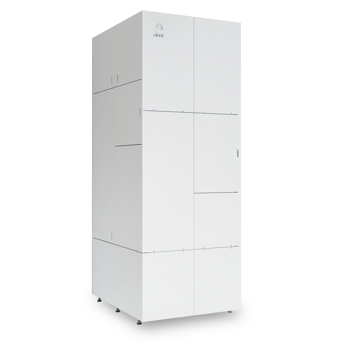
The JEM-Z200MF is an electron microscope with magnetic field-free objective lens which enables high resolution observation without applying strong magnetic field to specimens. Combined with a higher-order aberration corrector, atomic resolution imaging is possible.
Features
Magnetic field-free Objective Lens
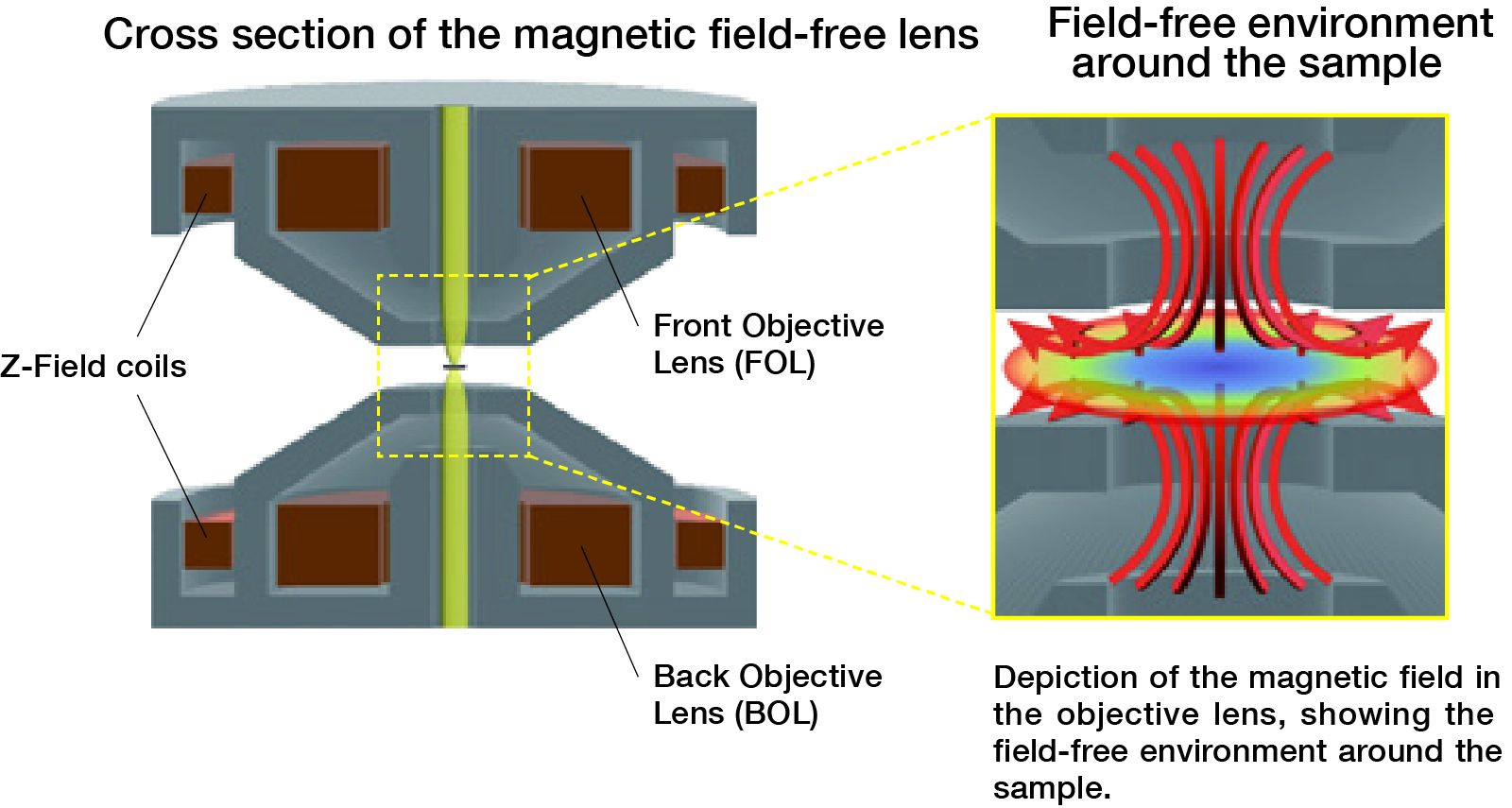
JEM-Z200MF objective lens consists of two lenses (FOL/BOL) located above and below the sample. The magnetic fields of these two lenses are canceled out at the sample plane, creating an objective lens with a field-free environment and a short focal length. The short focal length leads to low chromatic aberration and high overall stability. Combined with a higher-order aberration corrector, atomic resolution imaging is possible. A magnetic field in the Z-direction can be applied to the sample using built-in coils, located around the lens itself.
Double Corrector
The JEM-Z200MF is configured with Double corrector system on the illumination side as well as the imaging side, enabling both high-resolution STEM and TEM imaging.
Illumination System
The STEM corrector can be operated in two modes, one suitable for high-resolution observation, the other ideal for high sensitivity DPC investigations.
Large convergence angle mode
Ideal for high resolution observations.
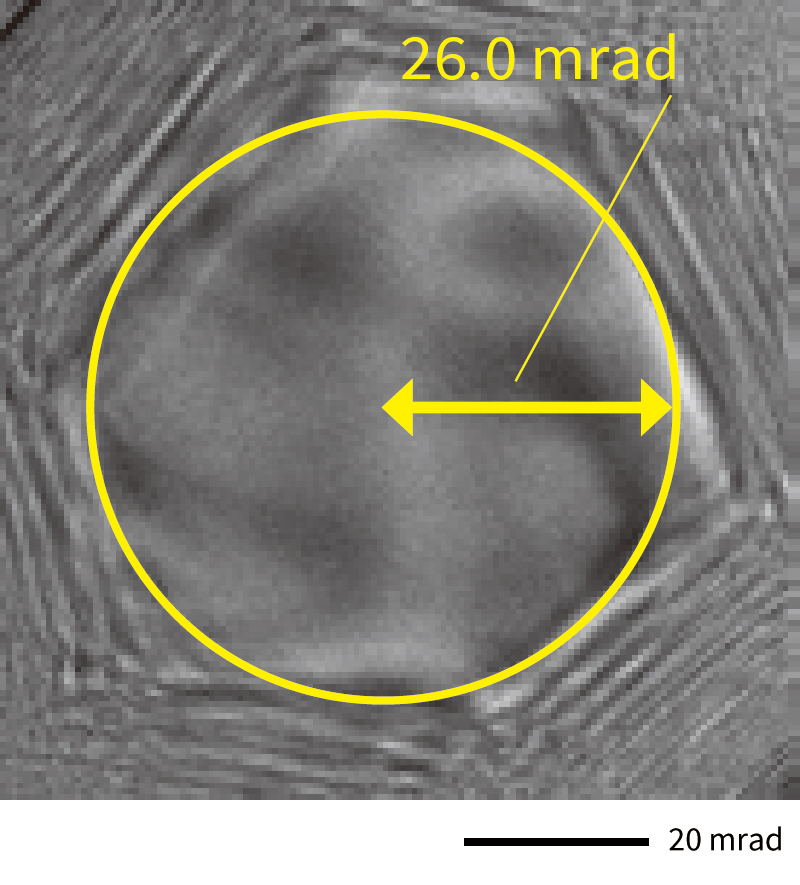
200 kV、MHRP
Convergence angle:
20 mrad (semi-angle)
( with 40 μm CL aper ture )
Small convergence angle mode
Ideal for DPC STEM observations.
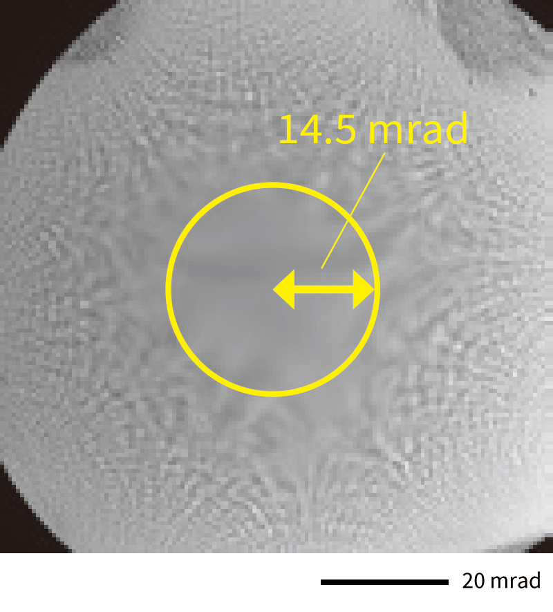
200 kV、MHRP
Convergence angle:
1.0 mrad (semi-angle)
(with 10 μm CL aper ture)
Imaging System
With the JEM-Z200MF, it is now possible to switch between CV(:Conventional) Mode for dark-field/bright-field observation HR(:High-resolution) Mode by pressing a single button.
Specifications
| MHRP*Configuration | MWGP*Configuration | ||
|---|---|---|---|
| Acceleration Voltages | 200 kV/80 kV | ||
| Electron source | Cold-field Emission | ||
| STEM Resolution | Bright-field | 0.092 nm | 0.136 nm |
| Dark-field | 0.092 nm | 0.136 nm | |
| TEM Resolution | Lattice Resolution | 0.09 nm | 0.10 nm |
| Information Limit | 0.14 nm | 0.16 nm | |
| Sample Tilt (X° / Y°) | Standard double-tilt holder | ±12° / ±16° | ±25° / ±27° |
| Magnetic field around the sample | 0.3 mT or less | ||
| Options | Energy-dispersive X-ray spectroscopy (EDS), Electron energy-loss spectroscopy (EELS), digital camera | ||
* MHRP : Magnetic field-free High resolution Pole-piece MWGP : Magnetic field-free Wide Gap Pole-piece
Catalogue Download
Please contact any of local offices.
Application
Visualizing electric/magnetic field distributions on an atomic scale
Differential Phase Contrast imaging (DPC)
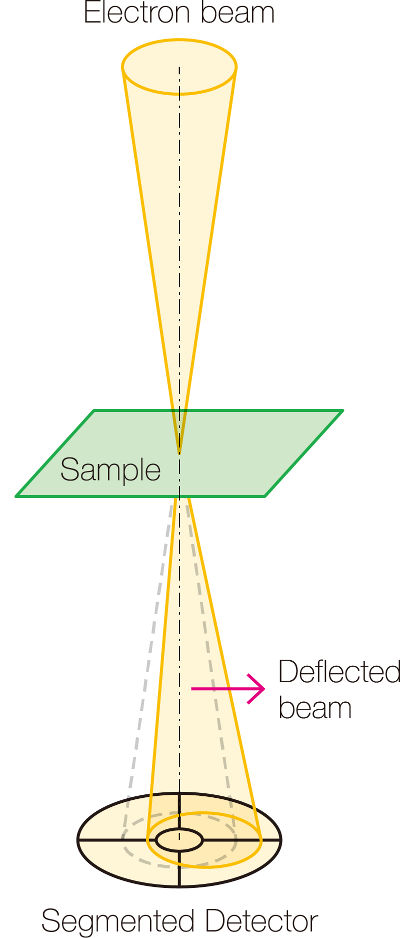
Electric and magnetic fields can be visualized using the DPC-STEM method, which measures the small deflections of the electr on beam due to the fields inside the sample with segmented or p ixelated detectors.
Principle of DPC-STEM
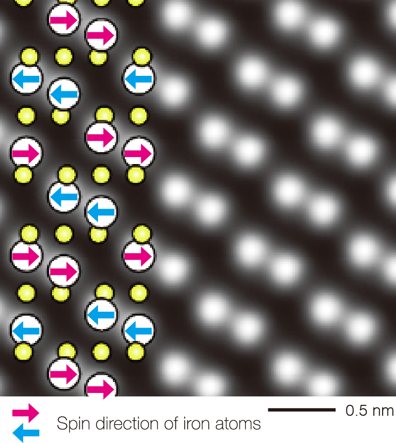
ADF STEM image
DPC STEM image
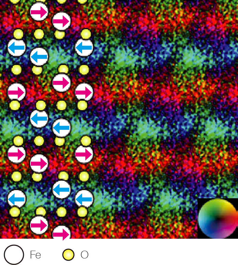
Observation of the magnetic field distribution (room temperature) of antiferromagnetic hematite at atomic resolution using DPC STEM.
The symmetry of the hematite crystal was used to remove the information about the electric field and the magnetic distribution was visualized by averaging over all unit cells. Colors indicate the direction and strength of the magnetic field.
Y. Kohno et. al, Nature 602, 234 (2022)
Reduction of diffraction contrast effects in DPC-STEM
Tilt-Scan system
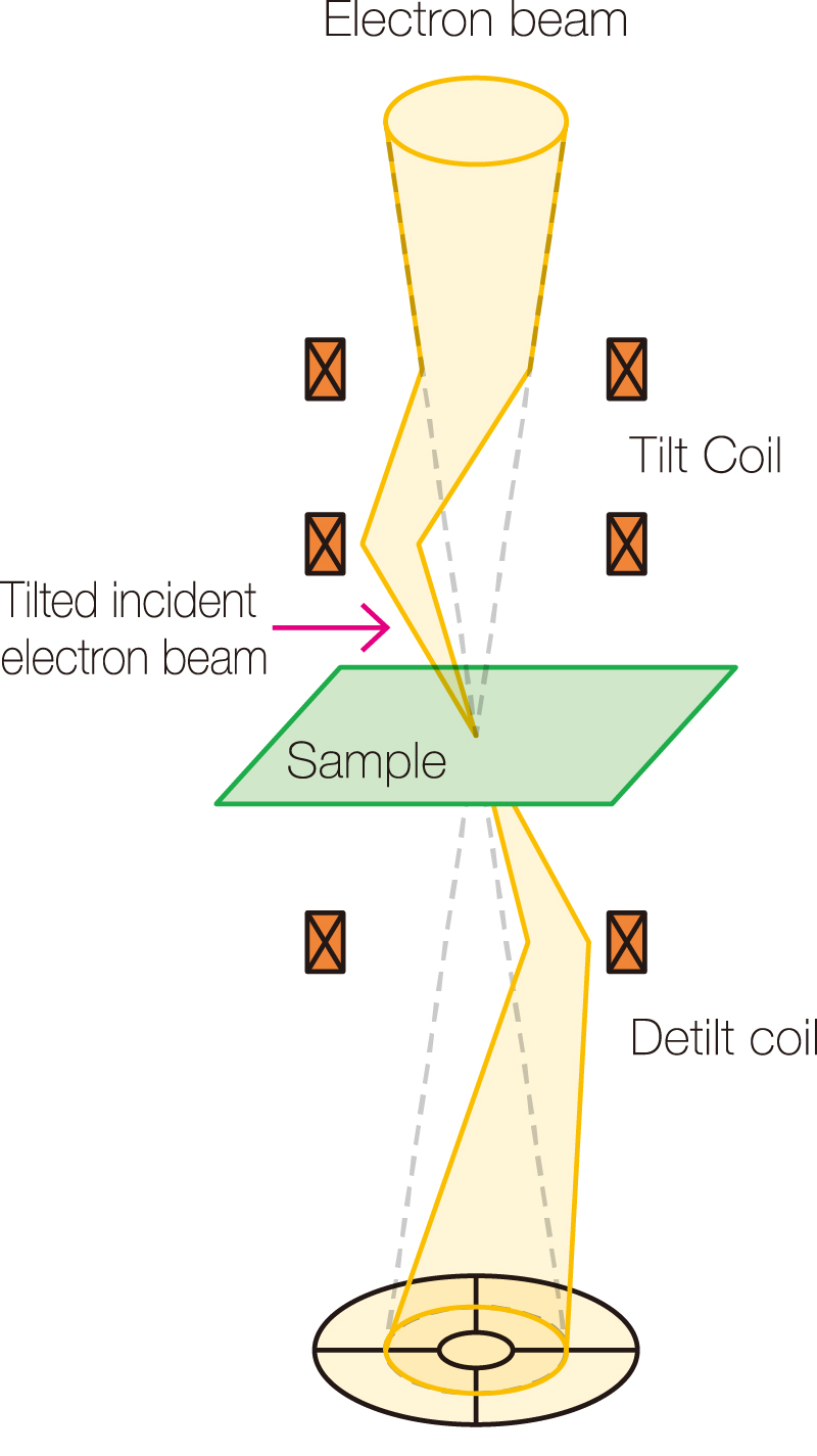
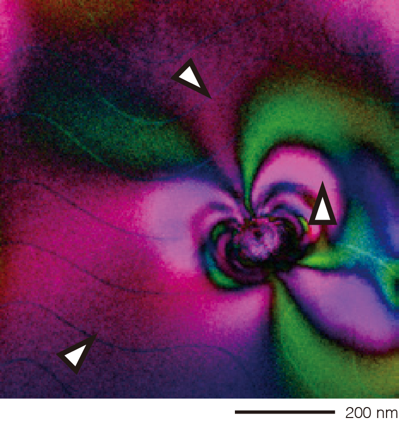
The JEM-Z200MF is equipped with a dedicated beam deflection system making it possible to change the incidence angle of the electron beam. Acquiring multiple DPC STEM images at different incident angles and then superimposing the individual images reduces the effect of diffraction contrast as shown below. (tilt-scan averaged DPC STEM, tDPC-STEM)
Principle of tDPC-STEM
Tilt scan OFF
Tilt scan ON
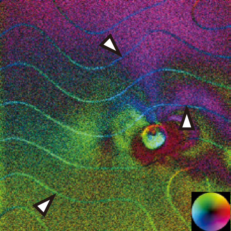
Comparison of DPC TEM image of Nd2Fe14B with and without the use of the Tilt-Scan system.
These images were observed along the axis of easy magnetization. Arrows in images indicate domain wall positions.
Using the Tilt-Scan system diffraction contrast caused by precipitates is strongly reduced and the domain wall boundaries can be clearly observed.
Gallery
High resolution STEM
The combination of the magnetic field-free objective lens with a probe side Double corrector system enables atomic resolution STEM under magnetic field-free conditions. The large convergence angle mode enables STEM observation with a high spatial resolution on the order of 0.1 nm.

HAADF STEM image of a Σ9 {221} symmetric tilt grain boundary of a Fe-3mass%Si bicrystal. The inset shows a unit cell averaged image of the grain boundary. By correcting the spherical aberration of the illumination system, it becomes possible to observe Fe grain boundaries.
T. Seki et. al, Incommensurate grain-boundary atomic structure,
Nature Communications 14, 7806 (2023), Fig. 1
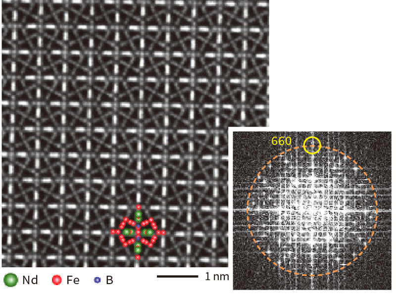
Neodymium Iron Boron magnet (Nd2Fe14B) High-resolution HAADF-STEM image taken along the [001] direction and corresponding FFT pattern.
The displayed orange circle corresponds to information transfer at 1Å. The STEM Image was formed by summing 30 drift-compensated images.
High resolution TEM in HR mode
The HR mode enables TEM observations at higher magnification under magnetic field-free conditions. Combined with an image side spherical aberration corrector, atomic lattice resolved TEM images can be obtained.
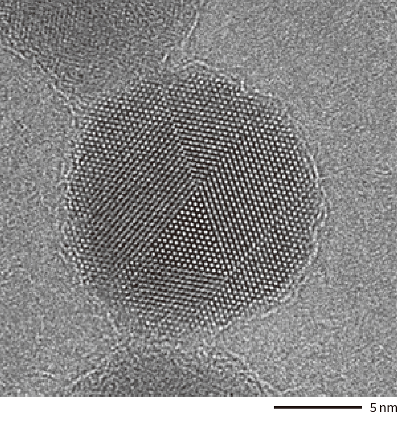
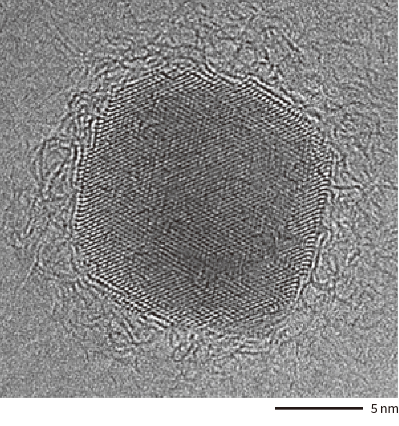
High-resolution TEM images of magnetite nanoparticles (Fe3O4).
By correcting the spherical aberration of the objective lens, the atomic arrangement of the magnetic particles can be studied.
Bright and Dark Field TEM image in CV mode
Linking physical and magnetic structural features is made easy by JEM-Z200MF. In the CV mode, the diffraction plane aligns with the objective aperture plane, allowing for easy selection of diffraction features to generate bright field and dark field images of magnetic materials.
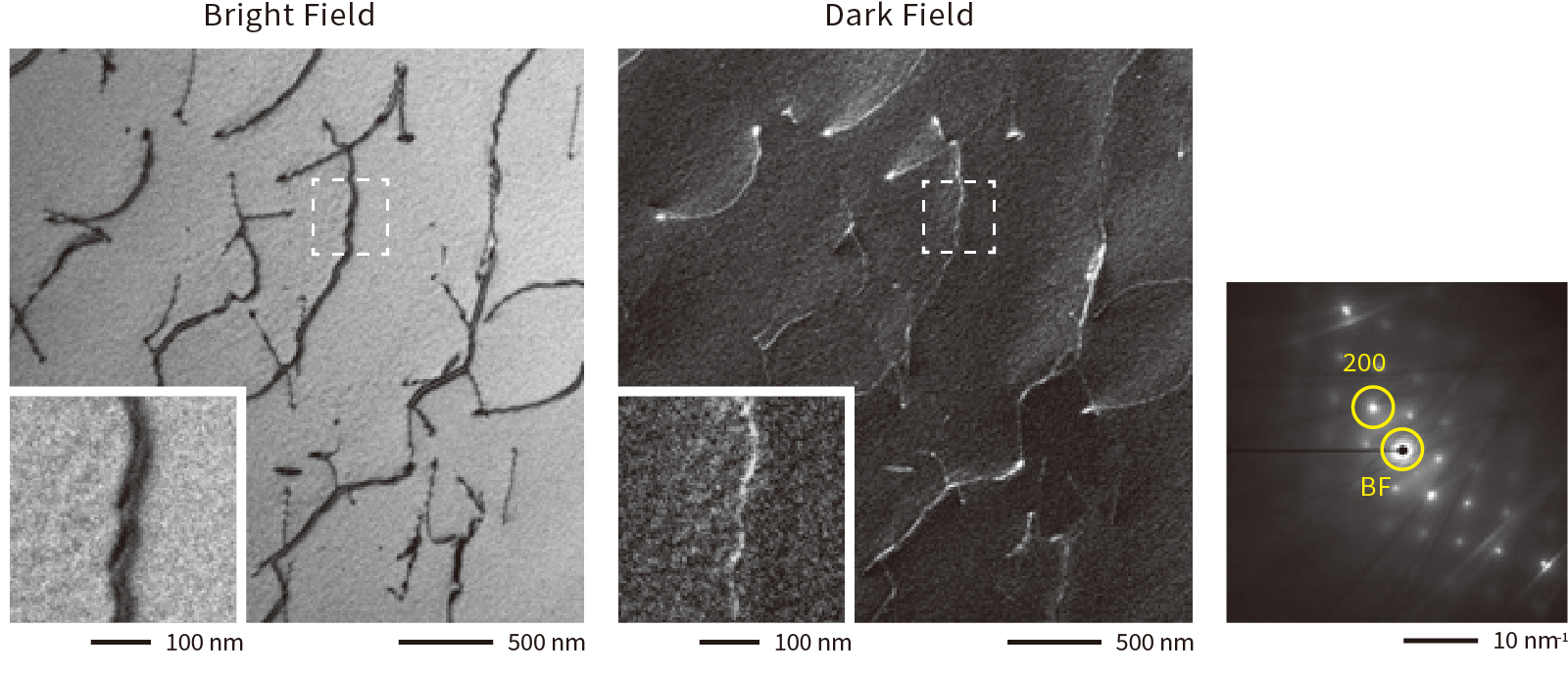
Bright-field and dark-field images of dislocations in a pure iron sample.
Dislocations were introduced by deforming the sample by 5% at liquid nitrogen temperature.
Yellow circles indicate the positions of the objective aperture. Incidence Direction: Near <001>
Data courtesy: Prof. Kazuto Arakawa, Shimane University
Lorentz-TEM / Fresnel method
Using a TEM with a conventional objective lens, it is necessary to turn off the objective lens in order to observe magnetic domain structures. With JEM-Z200MF, magnetic domains are easily observed with the objective lens normally excited.
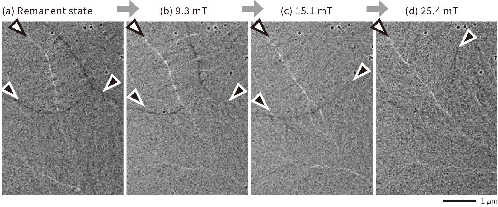
Under focused image / defocus value -800 μm
Observation of magnetic domains in a permalloy thin film (Fe22Ni78) using the Fresnel method.
Black and white arrows indicate the positions of domain walls.
Fig. a Remanent state of the permalloy thin film
Fig. b-d Using the magnetic field generating coils, which surround the objective lens, an external magnetic field is applied along the Z-axis.
Sample courtesy: Dr. Takumi Sannomiya, Tokyo Institute of Technology
Related Link
More Info
Are you a medical professional or personnel engaged in medical care?
No
Please be reminded that these pages are not intended to provide the general public with information about the products.
