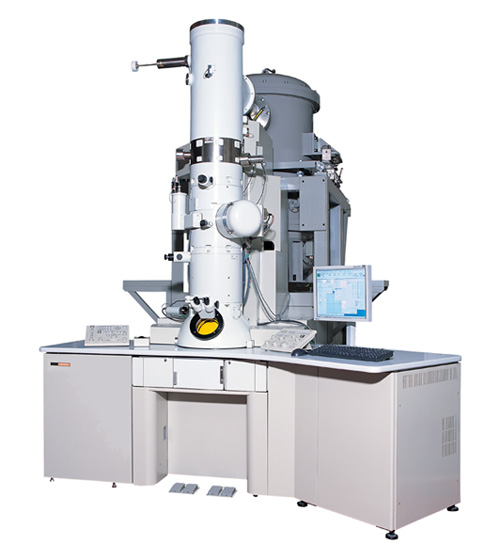
【DISCONTINUED】JEM-3100F 300 kV Field Emission Electron Microscope
DISCONTINUED
This product is no longer available.
If you would like to know the latest information about your preferred product or to find out more about alternatives, please click on the link below. We hope you will continue to use our products.
The JEM-3100F, a high-resolution, analytical electron microscope, can achieve sub-nanometer resolution imaging of structure and nanometer scale analysis of materials. State-of-the-art electron optical system of this microscope allows us to obtain a clear image with 0.1 nm resolution in both TEM and STEM modes. The JEM-3100F has improved mechanical and electrical stability, providing a stable electron beam even for a 0.14 nm probe. These features make the JEM-3100F a powerful research tool for analyzing materials at atomic level.
Features
Field emission gun (FEG)
Increase of the electron probe brightness on the specimen leads the improvement of S/N ratio in nano area analysis and observed images. FEG, which is employed for the JEM-3100F, provides approximately 2 order higher brightness than that with the LaB6 electron gun. With FEG, the contrast of high-resolution image is also improved because it provides a highly coherent illumination with a narrow energy spread. In addition, the electron holography that requires the highly coherent illumination is available for this microscope with an optional equipment electron bi-prism.
Condenser-objective lens*1
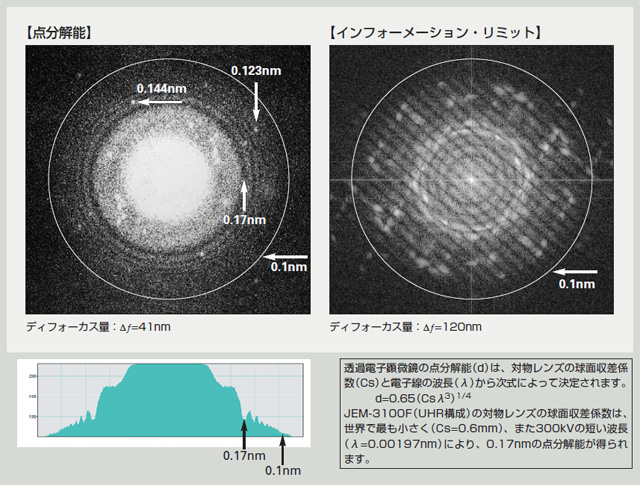
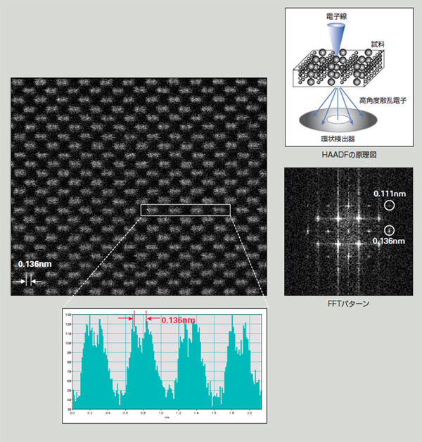
For reducing the probe diameter, small aberration coefficients for the illumination objective lens are required. The condenser-objective lens, providing functions of a condenser lens and an objective lens, can make the aberration coefficients small. The JEM-3100F employs a newly developed condenser-objective lens as its objective lens. This objective lens*2, besides offering the world's best level spherical and chromatic aberrations, 0.6 mm and 1.3 mm respectively, is designed with full consideration given to the optimum arrangement of the anti-contamination cold finger and EDS detector. As a result, elemental analysis and electron diffraction of specimen nanometer areas can be performed with a probe of 0.4 nm in diameter with a simultaneous ultrahigh resolution observation.
For UHR and HR configuration
For UHR configuration
New control type side-entry goniometer
The JEM-3100F employs a side-entry goniometer with a newly adopted servo-motor control, improving the operability of the specimen stage more than ever. Also, since the microscope provides a piezo-drive mechanism as standard, the operability of moving a field of view at a high magnification, drastically improves, when user switches to the piezo drive. In addition, the drift-free control device utilizing the piezo drive is available as an optional attachment. Furthermore, air-tight cover (Clam Shell) shielding the goniometer enhances the resistance against noise and atmospheric pressure variation.
Quick beam select system
The JEM-3100F provides wide range of illumination lens conditions. They are divided into the following four illumination modes:
TEM mode: For TEM image observation
EDS mode: For element analysis
NBD mode: For diffraction from an area of nanometers
CBD mode: For convergent beam electron diffraction
The optimum illumination mode can be selected for user’s purpose with a single touch of a button. While observing a TEM image, the desired microprobe can be obtained by a simple button operation to perform accurate micro area analysis.
Specifications
| Configuration※1 | Ultrahigh resolution(UHR) | High resolution(HR) | High contrast(HC) |
|---|---|---|---|
| Resolution | |||
| TEM particle image | 0.17 nm | 0.19 nm | 0.26 nm |
| TEM lattice image | 0.1 nm | 0.1 nm | 0.14 nm |
| STEM bright-field image※2 | 0.14 nm | 0.14 nm | - |
| STEM dark-field image※3 | 0.14 nm | 0.14 nm | - |
| Accelerating voltage | 300 kV,200 kV,100 kV※4 | ||
| Minimum step | 100 V | ||
| Electron source | |||
| Emitter | ZrO/W(100) Schottky | ||
| Brightness | 7×10⁸A/cm2・sr or more | ||
| Vacuum | to 3×10⁻⁸ Pa | ||
| Probe current | 0.5 nA or more at 1 nm probe diameter | ||
| Power-supply stability | |||
| Accelerating voltage | 2×10⁻⁶/min | ||
| Objective lens current | 1×10⁻⁶/min | ||
| Optical parameters for objective lens | |||
| Focal length | 2.7 mm | 3.0 mm | 3.9 mm |
| Spherical aberration coefficient | 0.6 mm | 1.1 mm | 3.2 mm |
| Chromatic aberration coefficient | 1.5 mm | 1.8 mm | 3.0 mm |
| Minimum variable focal length | 1.0 nm | 1.4 nm | 4.1 nm |
| Spot size (α selector) in nmφ | |||
| TEM mode | 2 to 5(3) | 7 to30(-) | |
| EDS mode | 0.4 to1.6(5) | 4 to20(-) | |
| NBD mode | 0.4 to1.6(5) | - | |
| CBD mode | 0.4 to1.6(8) | - | |
| Convergent electron diffraction | |||
| Convergent angle(2α) | 1.5 to20 mrad or more | - | |
| Acceptance angle(half angle) | 10 ° | - | |
| Magnification | |||
| MAG | ×4,000 to 1,500,000 | ×3,000 to 1,000,000 | |
| LOW MAG | ×60 to 15,000 | ||
| SA MAG | ×10,000 to 500,000 | ×6,000 to 300,000 | |
| Diffraction camera length | |||
| Selected area diffraction(mm) | 12 to 200 | 200 to 3000 | |
| High dispersion diffraction(m) | 4 to 80 | 4 to 80 | |
| Specimen chamber※5 | |||
| Specimen travel range(XY / Z) (mm) |
X,Y : 2 Z : 0.2 |
X,Y : 2 Z : 0.4 |
X,Y : 2 Z : 0.4 |
| Specimen tilt angle(X / Y) | ±25°/±25° | ±35°/±30° | ±38°/±30° |
| EDS※6 | |||
| Solid angle | 0.13 sr | 0.09 sr | |
| Take-off angle | 25° | 20° | |
Specify either configuration (UHR, HR or HC) when ordering the JEM-3100F.
To observe a STEM image, optional scanning image observation device is necessary.
To observe a STEM dark-field image, optional dark field image observation device is necessary.
To observe an image at 100 kV and 200 kV, optional electrode short switch is necessary.
The listed values are for the case when using specimen tilting Holder.
An optional EDS is needed. The listed performance is for the 30 mm2.
Gallery
More Info
Are you a medical professional or personnel engaged in medical care?
No
Please be reminded that these pages are not intended to provide the general public with information about the products.