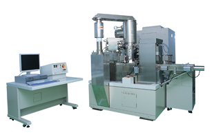
Electron Beam Lithography System
Pioneer in Ultra LSI Age
Semiconductor circuit components called LSIs (large scale integrated circuits) are built in electronic devices that we use daily, such as mobile phones, personal computers, game consoles, digital cameras, audio equipment, TVs, and so on. The latest LSIs are packed with more than one billion transistors. The electron beam lithography system (hereinafter: EB lithography system) is an instrument that plays an important role in the production and R&D of these semiconductor devices.
LSI-the magic wand of electronics
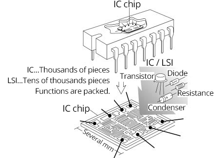
In 1945, the world's first electronic computer "ENIAC" (Electronic Numerical Integrator and Computer) was developed. About 18,000 vacuum tubes were used and the size was as large as 100 tatami mats room when all of the vacuum tubes are placed flatly. It was extremely heavy, as heavy as 30 tons. But today, with the appearance of the LSI, a computer with a performance of ten thousand times higher than the "ENIAC" became small enough to be carried about easily. This LSI, like a "magic wand" is a black plastic lump as large as a piece of caramel, with many legs like a centipede. Inside, there are 1 to 2 centimeters square thin plates. (These are called chips. This is exactly what makes it like a magic wand). On the chip, there are very fine circuit patterns that were designed according to the LSI function. And this very fine circuit pattern is drawn by the EB Lithography System.
How are LSI chips made?
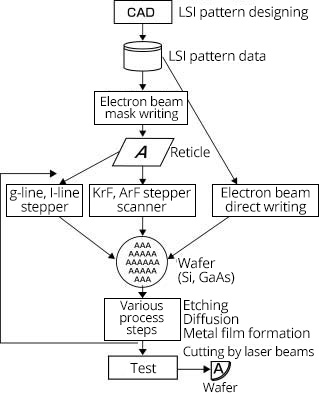
The LSI pattern designed for its purpose is exposed by electron beams to a quartz substrate (mostly 152 mm x 152 mm in size) with a chromium film coated with resist and a resist pattern is formed in the developing process. Etching is performed using this resist pattern as a protective film to form a light-shielding film of chromium. The resulting master plate is called a photomask (equivalent to a photographic film). Currently, the mainstream photomask is an enlarged photomask that is four to five times larger than the actual pattern on the LSI chip. The enlarged photomask is usually called a reticle.
The reticle pattern is burned onto the wafer using a light transfer device called a stepper or scanner. This is the same principle as that used in photographic printing. The reticle corresponds to photographic film, and the wafer corresponds to photographic paper. The major difference between the reticle and the film is that the circuit pattern on the reticle pattern is much finer than that on the film. The most advanced LSIs, such as DRAM (memory elements) and MPU (arithmetic elements), have extremely fine patterns with circuit line widths as narrow as 45 nm on a wafer.
The accuracy required for this 45 nm line width is capable of forming patterns on a material 152 mm x 152 mm square, of about 0.2 m line width (4 times of 50 nm) within dimensional and positional errors by about 2 to 5 nm. After pattern transcription, the wafers are developed, etched by using resist as a protective film, processed for diffusion, and the metal film is formed, etc.
The etching processes from pattern transcription are repeated several times to form the objective LSI chips. The LSI chips are cut into individual chips by laser beams and built in the package. The wafer is a silicon single crystal of 200 mm or 300 mm in diameter. Eventually, from this single wafer, several hundred LSI chips are created.
On the other hand, compound semiconductors such as high-frequency semiconductors used in the transmitter/receiver amplifiers of mobile phones and optical semiconductors that control the light source lasers of optical communications have a very thin circuit line widths of 0.1 m or less. And for this process only, EB lithography systems are also used to draw patterns directly on the wafer without using a reticle.
Freely Movable Electron Beam Pen
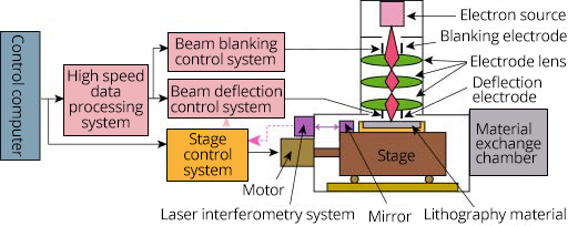
Structure of EB Lithography System
The figure shows a typical configuration of a spot beam system. Electron beams are emitted from the electron beam source, converged by an electron lens on the material to form a very small spot. On the other hand, the pattern data to be drawn is once stored in a hard disc provided with the computer used to control the instrument. This data is then transmitted from the hard disk to the blanking control system and beam deflection control system via a high speed data processing system. The beam is turned on and off in the blanking circuit to draw the pattern, and deflected to the designated position with the move of the deflector circuit. Patterns are drawn as designed, using a combination of the movements of electron beams and the stage. To accurately control the movement of the stage, a laser interferometry system is used. Such spot-beam systems are used for research and development of next-generation semiconductor devices by direct electron beam lithography and for production of high-frequency semiconductor devices and optical semiconductor devices. On the other hand, a variable shaped beam system is used for reticle production. This system is based on the concept of changing the beam shape from a spot to a rectangle and has made a breakthrough in high-speed lithography. In this method, the lithography pattern is divided into rectangles, which are then lithographed by a rectangular electron beam of variable sizes, as if stamping. This system is used daily at production sites as the main equipment for reticle lithography.