Electron Beam Source for Evaporation
What is an electron beam source for evaporation?
Electron beam deposition is to irradiate electron beams generated from the electron source in a vacuum to the evaporation material, then heat and evaporate it to form a thin film on substrates, lenses, and other objects to be deposited. Deflection electron beam sources which are placed in vacuum equipment, are used in a wide range of fields. Here, we introduce deflection electron beam sources. On the other hand, high-power electron beam sources which are large and with high power, capable of high-speed deposition, are used for a long film and large area substrate. Please refer to the technical information page for high-power electron beam source.
Overview of electron beam evaporation
Deflection electron beam source
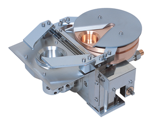
The deflection electron beam source consists of two parts. One is the electron beam source built into the vacuum evaporation equipment, which generates electrons and then accelerates and deflects them as electron beams. And the other is a crucible (hearth) section, which holds the evaporation material. Electron beam sources are also called E source, EB source, and E type electron beam source.
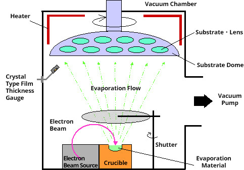
The following figure shows the image of the electron beam evaporation device.
Features of electron beam evaporation
Heating sources are the kinetic energy of electrons. Due to direct heating of
evaporation material, it is efficient.
Since the power density of an electron beam is large, enabling evaporation of various materials including
high-melting point metal, oxides, compounds, and sublimate. Electron beams can be controlled accurately in
electric fields and magnetic fields. High-speed scanning of electron beams in a certain range is possible,
allowing for beam irradiation with optimal power density for evaporation material. Electron beams are
deflected to either 270 degrees or 180 degrees and then irradiated to evaporation material.
It is used in a high vacuum (10-2Pa to 10-5Pa or so). Note: Ultra-high vacuum type is also available.
The use of more than one crucible and evaporation source enables the deposition of multi-layer film by
processing once.
Comparison of deposition methods and structure of electron beam source
Comparison with other deposition methods
The deposition rate is higher than the sputtering method or CVD (chemical vapor
deposition) method.
It can easily create a thick film of over 1 um.
Deposition of a high melting-point metal or metal oxide of high melting point is possible, which is not
possible (or difficult) with resistance heating method or induction heating method.
Since immediate heating and power change is possible by electron beams, precise film thickness control is
possible, which is difficult with a resistance heating method or induction heating method.
(Film thickness controller allows for control for desired film thickness or deposition rate)
Since evaporation materials in a water-cooled crucible are directly heated by electron beams, evaporation
materials are not contaminated by crucible materials. (Free from mixing of impurities or creating
alloys).※1
A resistance heating method or induction heating method may cause welding or reaction with an evaporation
boat or crucible.
Note 1. Even when an electron beam method is used, use of a hearth liner in a water-cooled crucible may cause welding or a reaction with the liner material. So, attention is needed.
Structure of Electron Beam Source
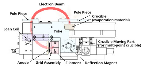
- The filament is energized and heated to emit heat electrons.
- Negative high voltage (normal -4 to -10 kV) is applied to the filament, accelerating thermal electrons with the voltage difference against anode.
- The electrons that jumped out are deflected in the magnetic field (by permanent magnet or electromagnet) and irradiated to the evaporation material in a crucible.
- Electric current is conducted to the scan coil as necessary to have the electron beams scanned to expand the irradiation area.
Fields of Application of Electron Beam Evaporation
Applications
1) Optical film/Oxide film
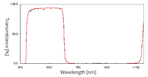
Optical thin films of various characteristics can be prepared by depositing and laminating metal oxide of different refractive indexes, including reflection proof film or filter film/mirror film that enables transmission or reflection of certain wavelength bands.
As one example, the characteristic when an infrared ray cut filter is deposited on a
glass substrate is shown.
It makes visible light transmitted and infrared rays reflected. Since it prevents infrared rays (hot wire)
from transmitting, it is also called a cold filter.
As an oxide thin film, it is also utilized for a protection film, insulation film, and transparent conductive film, etc.
[Examples of Final Product]
Eye-glasses, camera (digital camera/video
camera/mobile phone camera), LCD projector, Blue Ray/DVD/CD device, semiconductor laser, optical fiber, gas
barrier film, etc.
2) Metal film
In order to form electrode and wiring film for power devices and LED elements, low-resistance metal materials are deposited. Besides, it is used in decoration film, electromagnetic wave shield film, rigid film, and reflection mirror, etc.
[Examples of Final Product]
LED, semiconductor laser, power device, SAW (surface
acoustic wave) filter, organic EL, inorganic EL, lithium-ion battery, film condenser, console for PC and
mobile phone, watch/jewelry goods, tool, etc.