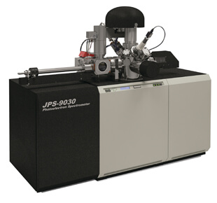
Photoelectron Spectrometer (ESCA)
Peeking into the micro world
X-ray Photoelectron Spectroscopy (hereinafter: XPS) has been used as a highly versatile analytical method in the research and development of materials, and for quality control. The photoelectron spectrometer is used in a wide range of applications, from Universities to factories, as a research tool with ease of operation that enables routine analyses.
History and Principle
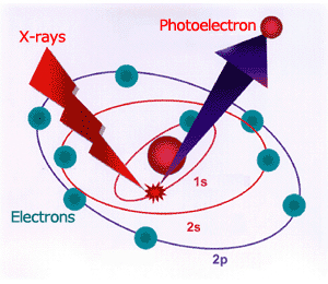
Fig.1 Principle of generation of photoelectron
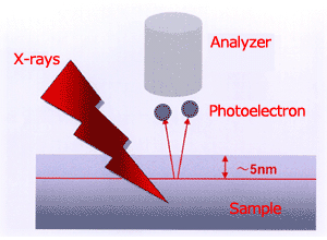
Fig.2 The escape depth of photoelectrons
Hertz discovered in 1887 that when a material is irradiated by light, electrons are emitted from the material. This phenomenon is called the Photoelectric Effect, and the emitted electrons are called photoelectrons since these electrons have been excited by the light. Einstein developed a hypothesis of light quanta in order to explain this photoelectric effect. Later, quantum mechanics was to evolve from this light quantum hypothesis.
In the 1950’s, Siegbahn in Sweden successfully performed energy spectroscopy of the photoelectrons emitted from a material, marking the start of energy spectroscopy as a useful method for surface analysis and chemical bonding state analysis.
Today, it is an indispensable surface analysis instrument for a wide range of applications, from research in areas such as metals, semiconductors, polymer compounds, and high technology materials, to product quality control.
Observation of Bonding States of Atom and Molecule
XPS is a method to observe a world even smaller than the one visible with an electron microscope. You may wonder “How can that be? How can we see anything smaller than an atom or a molecule?”. Of course, it is not like looking at a picture. Nevertheless, by measuring the speed of the electrons coming from inside a material when x-ray is irradiated onto the material (called photoelectrons because they are emitted when the material is exposed to light), it is possible to observe the tiny world inside an atom or a molecule.
Measuring the speed of these photoelectrons is called photoelectron spectroscopy, and determining the bonding state of atoms and molecules by analyzing the obtained spectra is called chemical state analysis.
Since it is possible to acquire chemical state analysis information, it is generally called ESCA (Electron Spectroscopy for Chemical Analysis)
In a sense, you could think of the photoelectron spectroscopy as the hardware, while state analysis is the software.
Chemical State Analysis
Guessing the dating partner from the clothing
An atom is composed of an atomic nucleus and electrons. The diagram of electrons revolving round the atomic nucleus like the planets orbiting the sun (Fig. 3(a)) is often seen. But in reality, electrons surround the nucleus like a cloud, rather than revolving in orbits (Fig. 3(b)). So, please imagine that an atom is clothed in electrons.

Fig.3 Model of the hydrogen atom
Now let’s think about our daily life. When you go to work, you may wear a work outfit. To visit a customer a sales person wears a suit, but on a day off, he/she may go out wearing a T-shirt. We wear the clothing that suits the situation and the circumstances. As a matter of fact, an atom exhibits similar behavior. An atom bonds (dates) with another atom to make a molecule. Depending on the dating partner, the atom changes the form of the outermost electrons to form the bond. To say it another way, if the dating partner changes, the clothing also changes.
Although it is not difficult to distinguish the clothing we wear, the differences in an electron cloud are not readily visible. It is necessary to peel off the electrons only. In other words, we have to remove the clothing by force. A method to remove the clothing without damaging it is the one called photoelectron emission. The differences in the electron cloud form can be observed as the differences in the speed of the electrons ejected from the atom by photoelectron emission. This is called the photoelectron spectrum (Fig. 4).
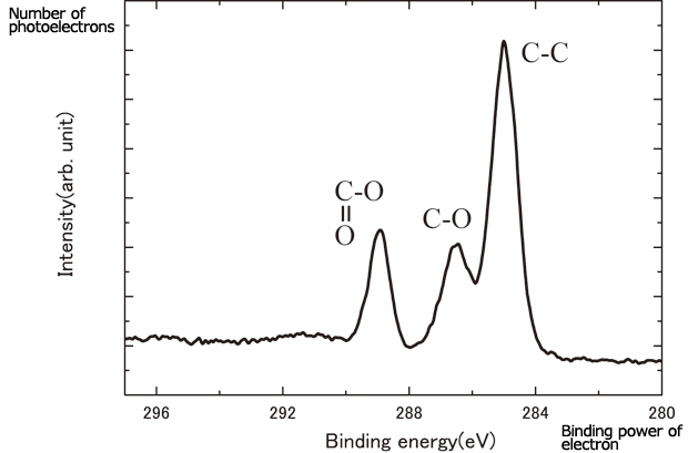
Fig.4 Photoemission spectra from polyethylene terephthalate carbon atoms
XPS to measure electron speed
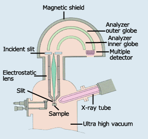
Fig.5 Diagram photoelectron spectroscopy
All the functions of a photoelectron spectrometer (Fig. 5) are housed in an ultra-high vacuum container; and the system consists of an X-ray generator (X-ray tube) to emit photoelectrons and an electron spectrometer to measure the speed of electrons. The electron spectrometer is composed of a series of electrostatic lenses and a hemispherical sector analyzer, as well as detectors. First, the electrostatic lenses slow down the speed of the electrons to improve resolution. Next, the analyzer selects electrons of a certain speed only.
The selected electrons are conducted into the detector, and the number of ejected electrons is counted. The number of detected electrons roughly corresponds to the number of atoms which compose the material or substance. To prevent the material surface from becoming contaminated and to prevent interference with the electron emission from the specimen, the photoelectron spectrometer is kept in an ultra high vacuum.
By analyzing spectra obtained in this way, the bonding state of an atom can be determined.
Characteristics
(1) This is a surface analysis instrument to analyze to a depth of several nanometers beneath the specimen surface.
(2) It can provide qualitative and quantitative analyses from Li to U, chemical bonding state analysis as well as photoelectron image measurement.
Application Example of Photoelectron Image
Photoelectron image of multi-layer structure in DVD-RW
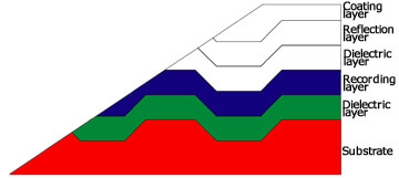
The commercially-available DVD-RW discs generally have a structure like the one shown in the figure on the right. When the surface of a DVD disc is stripped, the recording layer and dielectric layer will be exposed. As a result of acquiring photoelectron images while 3 kinds of layers are exposed, the data shown in the following figures were obtained.
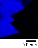
Photoelectron image Sb
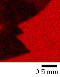
Photoelectron image C
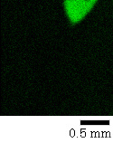
Photoelectron image Zn
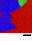
Sb, C, Zn superposition
(3) With regard to the materials that can be examined, analysis is possible even of insulating materials and conductive materials, such as polymer films, semiconductors, ceramics, and metals.
(4) By using an inert gas ion beam such as Ar ion, composition distribution analysis from the surface to the interior of the material (depth profile analysis) is possible.
Application Example of Depth Profile Analysis Specimen: (SiO2/TiO2) multilayer film/glass
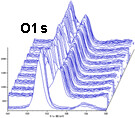
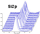
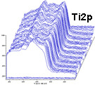
(Photoelectron spectra in the depth direction)
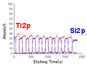
(Composition profile in the depth direction)
(5) As a method to obtain the composition and chemical bonding state changes from the top surface to several nm beneath the surface, a specimen tilt method (Angle resolved XPS, ARXPS) is available. This method is characteristic to XPS, and it can be used to measure the composition and chemical bonding state changes of the surface at a nano-order.
(6) The detection limit is about 0.1 Atomic% or so on average.
Necessities for technical reform
The applications of XPS can be classified into 3 categories.
The first is academic use. It is used for a wide range of applications, from surface research, research of electron structure in an atom such as band structure of semiconductor, to the research of complex salt chemicals, and even for studying the prevention of tooth decay.
Second, it is utilized for new product development and improvement of production technologies. It is used not only in metal and semiconductor industries, but also in analysis of particles and insulating materials, such as for catalyst industries and glass, and for organic materials such as polymer film, etc.
Thirdly, it is used for product quality control of mass production at factories, such as manufacturing process control for hard disc lubricant film thickness, semiconductor surface contamination, etc. as well as for failure analyses, such as analysis of the causes of corrosion, discoloration, oxidization, and so on.
Photoelectron spectrometers are playing an active role as the ideal instrument to satisfy the requirements in various fields when equipped with a wealth of additional functions.