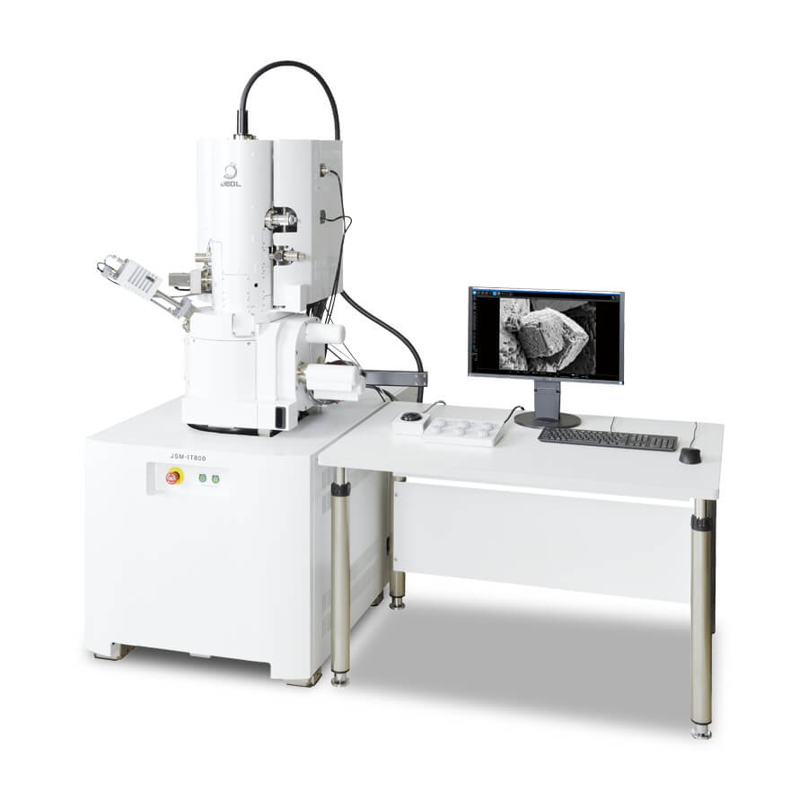
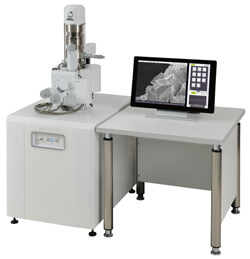
Scanning Electron Microscopes (SEM)
Scanning Electron Microscope
The champion of micro surface observation
The first step of a scientific evaluation is to thoroughly observe the form of the material. For this purpose, we have a magnifying glass or an optical microscope. But, as long as light is used, we can’t see anything smaller than the wavelength of light and therefore observing a nano structure is extremely difficult.
The Scanning Electron Microscope (SEM) introduced here utilizes an electron beam whose wavelength is shorter than that of light and therefore observing a structure down to several nm in scale becomes possible.
1nm = billionth = 10-9m
Scanning Electron Microscope → SEM
The Scanning Electron Microscope, which is utilized in various fields such as medical, biological, metals, semiconductors and ceramics, is broadening its application frontier. With abundant attachments and devices being combined, its capability is expanding. SEM is regarded as one of the most powerful tools being used at R&D institutes and quality control inspection sites all over the world.
Observation of the micro world using electrons
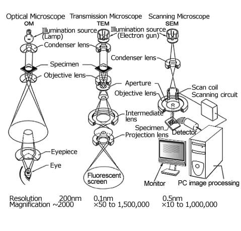
The Scanning Electron Microscope (hereinafter “SEM”) enables a clear observation of very small surface structures, which is not possible with an optical microscope (hereinafter “OM”). Moreover, as it can provide images with deeper focal depth, it enables observations of 3-dimensional images, with a similar sense as when we look at a substance with the naked-eye, by enlarging the specimen surface which has a rough structure.
SEM utilizes electrons to show an enlarged image of a specimen, in the same way as the transmission electron microscope (hereinafter “TEM”). Since an electron has a shorter wavelength than light, it enables us to observe smaller things than can be seen with the OM. The word resolution refers to the smallest size that can clearly be observed (the shortest distance between two neighboring points…the resolution of the human eye is said to be 0.2mm). The TEM’s resolution is 0.1 to 0.3nm while the SEM’s resolution is 0.5 to 4nm. The reason the SEM’s resolution is lower than the TEM’s is attributed to the fact that the wavelength of the electrons becomes longer because the accelerating voltage of the electrons used in the SEM is as low as several kV to several tens kV, and to the characteristic difference of the electromagnetic lenses used to converge the electron beams.
TEM provides an enlarged image projected onto a fluorescent screen, where the image is formed by the electrons transmitted (passed) through the thinly prepared specimen. In comparison, SEM forms the image using the electrons which were reflected or generated from the surface of the specimen.
Why can a specimen be observed with an electron?
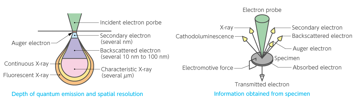
From the spot illuminated by the electron beam, various signals, such as secondary electrons, backscattered electrons, characteristic X-rays, and cathodoluminescence, are emitted depending on the form of the specimen, the density of the substance, and the elements contained inside.
The Scanning Electron Microscope (SEM) normally detects secondary electrons to form an image for observation. As the intensity of the generated secondary electrons varies depending on the angle of the incident electrons onto the specimen surface, subtle variations in the roughness of the surface can be expressed according to the signal intensity.
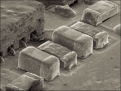
Cases observed (sample : implemented board)
Clear 3D images with easy operation
Now, let’s take a look at the process of observing an image by taking a biological specimen as an example.
A biological specimen needs a pre-treatment called specimen preparation. This is essential to protect the vulnerable specimen from damage due to the heat caused by the electron beam shower. In addition, a specimen like biological tissue that contains water must be dehydrated before being mounted in the specimen chamber, which is kept at a high vacuum. The specimen is dehydrated after chemical fixation to prevent deformation when the water is removed, and is fixed to the specimen mount with a special paste or adhesive tape. Then, the entire specimen surface is thinly coated with metal particles such as Au or Pt-Pd using the techniques of sputtering or vapor deposition. The metal coating prevents a charge from forming on the specimen surface, and increases the secondary-electron yield, which consequently contributes to obtaining sharp image-signals. After the specimen preparation is complete, the specimen stage is fixed to the specimen movement stage in the specimen chamber and then the chamber is evacuated. The evacuation is automated and completed in one minute.
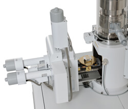
Now you are ready to operate the instrument to make an observation. It is so easy that no special qualification, such as a driver’s license, is required. Set an accelerating voltage of 20kV, for example (about the same electron energy as a color TV). Higher accelerating voltages give better resolution, but the damage to the specimen also increases. If you want to observe the surface of the specimen with very little damage, a low accelerating voltage, like several kV, should be used. Next, heat the filament to emit electrons. They are focused into an electron beam by adjusting the magnetic field lens using the control knob. Some instruments are equipped with an auto focus function. Next, adjust the magnification. You identify the area of your interest by searching at low magnification, and then you can raise the magnification gradually to display and record the enlarged image.
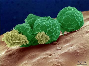
As seen in the right photo, the deeper focal depth than optical microscopes allows the SEM to create clear, 3-dimensional images.
This photo was taken by a low vacuum SEM and processed with pseudo color.
Photograph:
Courtesy of Prof. Takashi Tsuruhara and Mr. Hidehiro Kasahara - Tokyo Gakugei University, Biology
(Au coating, after freeze-drying in the sample tube following the fixation/dehydration)
Great performance for surface observation and analysis
There are many types of scanning electron microscopes, ranging from the ordinary type which uses a tungsten filament as an electron source, to the more specialized type which, with the field emission electron gun mounted, attains higher resolution and magnification.
By adding attachments such as the X-ray detector for elemental analysis, the backscattered electron detector for observing the composition, and the EBSD (electron backscattered diffraction) for crystalline analysis, it is possible to further expand the measurement versatility.
Various Function of SEM
| Secondary Electron Image Observation | Secondary electrons are used to observe the topography of the specimen surface. |
|---|---|
| Backscattered Electron Image Observation |
Backscattered electrons are mainly used to observe the compositional differences of the specimen. In the case of a polycrystalline specimen, the differences in crystal orientation are observed as the contrast in the image. (channeling contrast) |
| Absorption Electron Image Observation | Absorbed electrons are mainly used to observe the compositional differences of the specimen. The contrast is the reverse of that for the backscattered electron image. |
| Transmission Electron Image Observation | Electrons transmitted through a thin film layer are used to observe the differences in composition and density. |
| Cathodoluminescence(CL) Image Observation and Spectrum Analysis | The light emitted from a specimen stimulated by electron beam irradiation forms an image, and an emission spectrum is created a by means of wavelength spectrometry. This is used for applications such as the evaluation of impurities and defects in semiconductors, the evaluation of stress distribution, the evaluation of defect structure distribution in the oxide film, the evaluation of light emitting elements, etc. |
| EDS(Elemental)Analysis | This is a function to obtain a spectrum of the energy intensity of X-rays using a combination of the Li- doped Si semiconductor detector and the Multi-Channel Analyzer (spectrum analyzer). All elements from B to U can be detected and measured simultaneously. Even with the modest probe current, which decreases the risk of specimen damage, it performs excellently in the micro area analysis. |
| EBSD Analysis | Backscattered electrons which have been diffracted on a specimen surface are used to identify crystal orientation in a micro area and to measure the orientation map. |
| WDS(Elemental) Analysis | This is a function to obtain a wavelength spectrum by utilizing the diffraction phenomenon of X-ray by a crystal. Its features are high energy resolution and high detection sensitivity. |
| EBIC Measurement, Observation | The electromotive force (EMF) generated inside a specimen due to irradiation by an electron beam is used for defect analysis of semiconductor devices. |
| Low Vacuum Function |
A function to set the pressure in the specimen chamber to several tens to several hundred Pa. Decreasing the vacuum in the specimen chamber reduces the occurrence of charging. This makes it possible to observe a non-conductive specimen without the need for a difficult pre-treatment (coating). It is used for specimens with a lot of outgassing, specimens with a low vapor pressure, and specimens containing water as well. |
| Electron Beam Exposure Function | Resist lithography by electron beam is possible. |
| Cryo SEM Observation | Observation of a water-containing specimen is possible by freezing the water. This can prevent deformation of a specimen from occurring during the processes of fixation and dehydration. |
| Heating Observation |
Observation while heating a specimen is possible. Changes occurring to a specimen caused by heat such as swelling and segregation of impurities can be observed. |
| Tensile Observation | Observation while stretching a specimen is possible. This is used to observe the starting point of ductile fractures and analysis of material strength. |