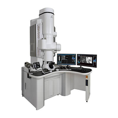
Transmission Electron Microscope (TEM)
Transmission Electron Microscope
Using Electrons to Explore the Micro World
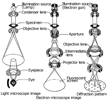
To satisfy this curiosity, many inventions have been devised. One of them is the optical microscope. The human eye can distinguish objects down to about 0.2 mm. Optical microscopes reveal small objects, which would be otherwise invisible to the human eye, by magnifying them with the help of a combination of glass lenses. If we raise the amplification rate (magnification) of an optical microscope higher and higher, can we see an atom? Unfortunately, the answer is “NO.” Optical microscopes use light as the illumination, so they have a limited ability to distinguish small structures (resolution). They cannot distinguish any structure smaller than the wavelength of light.
Engineers, like Ruska in Germany, broke this limit. They invented the “electron microscope”, which uses an electron beam as the illumination source instead of light. That enables us to observe small structures at a far better magnification than is possible with optical microscopes. It is now possible to distinguish the arrangement of atoms in materials.
Electron microscopes enable clear observation of micro-structures, which is not possible with optical microscopes. Moreover, they also make it possible to analyze substance structures and obtain atomic level information by using an electron beam. The electron microscope is an epoch-making invention used throughout the world to investigate an atomic world that we could hardly imagine.
The difference between Electron Beam and Light
A characteristic of electrons is that they cannot move freely in the air. They can, however, move freely in a vacuum. For this reason, a vacuum is maintained inside the column of an electron microscope; something that is not required for an optical microscope.
A specimen is illuminated by a beam of electrons accelerated by a device called an electron gun. These electrons either penetrate the specimen or cause scattering. By selectively converging and diverging these electrons with an electron lens (electric and magnetic fields deflect the electron beam to form images, in the same way the glass lenses deflect the light for the optical microscope), the enlarged images are formed on a fluorescent surface which is positioned below the beam and specimen.
Electron beams are flows of electrons generated in the vacuum by heating or by applying a strong electric field to a fine filament, and have the nature of a “wave”, with a wavelength shorter than that of visible light. Instead of glass, the lenses of an electron microscope are a combination of electromagnets constructed to form magnetic field lenses.

fig1. Ripples caused by the difference in the magnitude of the wave
As explained above, the ability to distinguish a small structure, that is resolution, largely depends on the wavelength of the “wave” used to illuminate the specimen.
The nature of this “wave” may be easily understood by comparing it to the wave pattern arising when a small stone is thrown into a lake. Assume the waves on the water surface come into contact with a rock protruding above the surface. If the rock is larger than the length between the crests of the waves (wavelength), then the wave pattern does not continue behind the rock (Fig,1). This creates a shadow. If the rock is smaller than the wavelength, however, the wave pattern will not be interrupted behind the rock and there is no shadow. In this case, the existence of the rock cannot be detected.
Whereas the wavelength of visible light is 400 to 800 nm (1 nanometer is one 100,000th of 0.1mm), the wavelength of the electron beam, which is used as a light source in the electron microscope, varies depending on the accelerating voltage. The accelerating voltages commonly used are 100 to 200 kV (corresponding to wavelengths of 0.0037nm to 0.0025nm).
This wavelength is far shorter than that of light, and sufficient to distinguish the arrangements of atoms (several nanometers). For the optical microscope the combination of the lens is varied to alter the magnification. In contrast, for the electron microscope, the intensity of the electric current passed to the electromagnets is varied to change the intensity of the magnetic field. This corresponds to the changing the thickness of a convex lens. In fact, by manipulating the electric current, the magnification can be freely controlled.
Another characteristic “electron diffraction”

Another great feature of the electron microscope is that an electron diffraction pattern can be obtained.
This is important information which reveals the nature of materials (specimen), especially, its atomic arrangement. Similar information can be obtained using an X-ray, but it lacks correlation with the image of the irradiated area. Electron microscopes allow images to be observed at a high magnification and diffraction analysis at a nanometer scale to be performed for the same irradiated area.
Electrons used to illuminate a very thin specimen, will be scattered while penetrating it. This process gives an electron diffraction pattern and the electron diffraction method can reveal the arrangement of molecules and atoms in a crystalline specimen. This technique is playing an important role in the field of material science.