Analytical Electron Microscope
Analytical Electron Microscope
JEOL presented the world’s first analytical electron microscope in 1970, at the 7th International Conference of Electron Microscopy (Grenoble, France). Since then, thousands of units have been used at top-notch universities and institutes around the world. Analytical electron microscopes have become a tool for not only observing nano-scale structures, but also for capturing information on the interaction between the incident electrons and the atoms of the specimen. As a result, the application of the electron microscope has dramatically expanded. Today, there is no transmission electron microscope that can’t be equipped with analytical functions. They are valuable tools in cutting-edge fields, such as scientific research and material development.
From “Wanting to see” to “Wanting to understand”
The idea of the microscope, which was born from our strong desire to see small things clearly, has evolved from the optical microscope in the 17th century into the electron microscope. Although the electron microscope appeared only 50 years ago, at present, it has advanced to the degree that our atomic and molecular world can be directly observed. Our desire to see small things is being satisfied to an extreme level.
However, our scientific desire is infinite; we are keen to know what exists inside what we have already seen. This might be the same desire since the dawn of science; we have evolved using our senses of smell, hearing, touch and taste to learn about the things we see.
Analysis of every kind of data
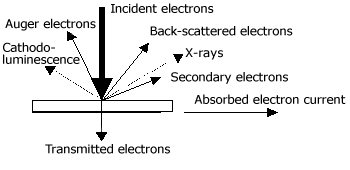
fig.1
An analytical electron microscope is a transmission electron microscope equipped with analytical functions such as EDS (energy dispersive X-ray spectrometry) and EELS (electron energy loss spectrometry), to enable qualitative and quantitative measurements, elemental distribution mapping, and chemical state analyses in the micro-size observation areas.
When a specimen is illuminated with the accelerated electrons, equivalent to the light of an optical microscope, various phenomena occur. As shown in Fig.1, various signals reflecting the nature of the specimen are generated.
By detecting the secondary electrons and the backscattered electrons the instrument functions as a scanning electron microscope for observing the form and structure of the specimen’s surface. This makes it possible to obtain an image with better spatial resolution (the shortest distance between two neighboring points that are distinguishable) than the conventional single function scanning electron microscope.
By measuring the intensity of the characteristic X-rays emitted from the specimen, the composition of elements in the specimen can be identified. This method is called EDS, a different technique from the EPMA method (wavelength dispersive X-ray spectrometry used in the electron probe micro analyzer), which examines the wavelength of characteristic X-rays with the aid of dispersive elements.
EDS employs a semiconductor detector where lithium is diffused on silicon. Energy from a characteristic X-ray which was generated from a specimen is immediately converted by this detector into the voltage pulse corresponding to its intensity. By counting the number of pulses of each size, the elemental analysis and the calculation of the composition ratio can be carried out.
By detecting the transmission electrons, it is possible to obtain not only the high resolution electron microscopic image, but also the scanning transmission image and the electron beam diffraction pattern that reflects the crystalline structure.
The transmission electrons include both the electrons which resulted from the interaction of the incident electrons with the atoms of the specimen as well as electrons which did not undergo such interaction. Using this fact we can make an elemental analysis and track down the chemical bonding state and the atomic distance of the specimen by measuring the intensity of the energy of the transmission electrons. This method is called EELS and is regarded, along with EDS, as one of the important functions provided by analytical electron microscopes.
Especially Good for Analysis in Micro Areas
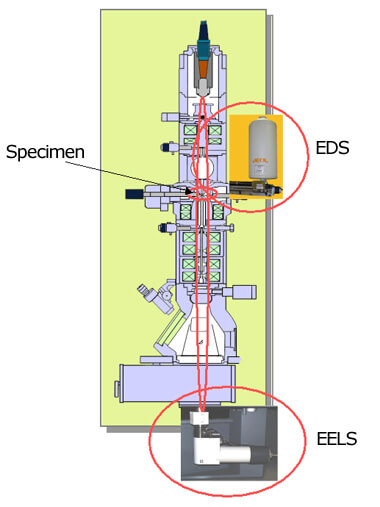
fig.2
The structure of an analytical electron microscope is as shown in Fig. 2.
By adding the functions of a scanning electron microscope onto the basic unit of the conventional transmission electron microscope, surface observation of a specimen becomes feasible.
Analytical electron microscopes can utilize various signals to form images. Simultaneously, the incorporation of EDS and EELS enables elemental analysis and the observation of energy loss images.