Auger Electron Spectroscopy
Auger Electron Spectroscopy
Seeker of nanostructures and thin films
An Auger Electron Spectroscopy is a very useful instrument for clarifying the various phenomena related to material surfaces. There are many unknown areas in this field, and the obtained information is very interesting by itself. At the same time, it is indispensable for material development. Further application in an even wider range of fields is expected in the future.
When a narrowly-focused electron beam is irradiated onto a material surface, electrons will be ejected from the very top surface of the specimen; the ejected electrons are called Auger electrons. This is an electron which has energy unique to the source element, and by measuring the energy of the Auger electrons, it is possible to determine which elements exist, in what kind of chemical situation, in a very small area of the top surface of a solid. By examining the intensity of the emissions, it is possible to determine, how much of each element is present.
Auger Electron Ejection from an Atom
Let's explain what the Auger electron is, which holds the key for structural analysis of a material surface.
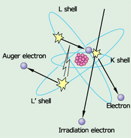
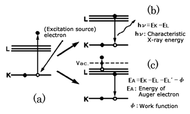
Fig.1 Auger electron generation principle diagram
As shown in Fig. 1, an atom has electrons around the nucleus. A fixed number of electrons fill in the places in each level, which are named the K level, L level and so on. In addition, the energy of the electrons is higher in the levels that are further away from the nucleus, increasing in order of the K, L, and M levels.
Also, the energy of an electron in each level, K, L, M, and so on, is a specific value for each element.
Now, when a high speed-electron flies from the outside into an atom, it may collide with an electron in the K level and knock it outside of the atom (fig. 1(a)). This means the K level is now missing one electron, so one of the electrons from the L level will move to fill the gap. This is because an atom always acts to achieve a stable state having the lowest energy. If an electron in the L level, which has high energy, drops into the K level, which has a lower energy, then there is extra energy left over. This extra energy can be emitted from an atom in two ways, as follows.
(1)Forming X-ray and emitting energy (Fig. 1(b)).
(2)An electron in the L level obtains the energy and is ejected (Fig. 1(c)).
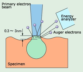
Case (2) is called a KLL Auger transition, and the ejected electron is called an Auger electron. This is named after P. Auger, who first discovered this phenomenon.
The energy of this Auger electron will be the difference between the energy of an electron in the L level and the energy of an electron in the K level minus the energy required to make the jump outside the atom. This value is unique to each type of atom, and is about several 10eV to 3000eV. The distance that an electron with this level of energy can move in a solid without losing energy is no more than several nm (nanometer: one-millionth mm). If an Auger electron is emitted from a location below the surface of a solid, it will lose energy as it travels through the solid, and can never be ejected from the surface. Therefore, Auger electrons are only emitted from the very uppermost surface. This is the reason the Auger Electron Spectroscopy is an instrument for surface analysis.
What kind of data is obtained by what kind of instruments?
Now, we will explain the instrument mechanism.
The electron beam emitted by the electron source passes through a lens, and is collimated, then irradiated to the specimen surface.
By scanning this focused electron beam on the specimen surface by using a deflector coil, the user can select the area of interest, or observe the Auger image.
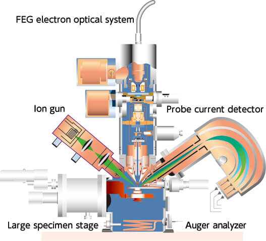

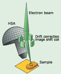
Fig.2 Principle diagram cross-section and JAMP-9500F
Auger Spectrum
The electrons emitted from the specimen surface are analyzed by an instrument that differentiates energies, called an HSA (hemispherical sector analyzer). After the voltage to apply to the HSA is determined, only the electrons which have the energy corresponding to the voltage will be able to pass through the HSA and be detected.
Therefore, if we check the amount of detected electrons while scanning the voltage applied to the HSA, we can detect Auger electrons which are mixed with secondary electrons and backscattered electrons. By examining the peak energy, we can determine what elements exist on the specimen surface. Since the background from the secondary and backscattered electrons is large and the Auger peak is small, to make Auger peak easier to observe, the detected electron spectrum is differentiated and displayed. The horizontal axis is the energy of the Auger electrons while the vertical axis represents the quantity of Auger electrons. Fig. 3 shows the Auger spectrum.
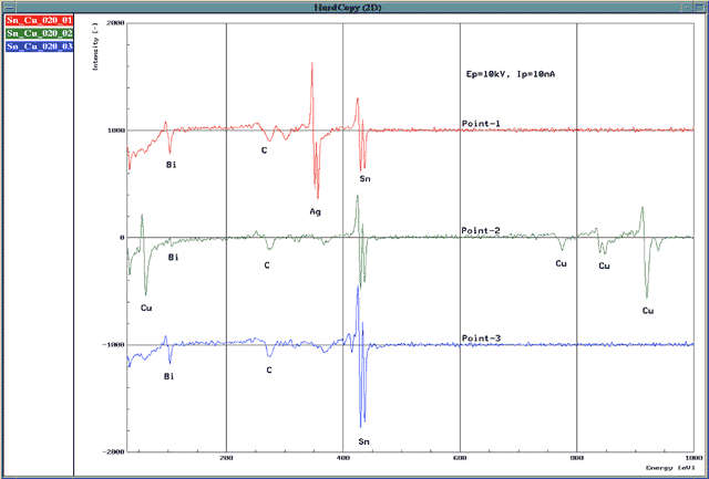
Fig.3 Auger spectrum system Sn · Ag · Cu · Bi (Pb-free solder)
Including scanning electron microscope functions
When electron beams hit a material, electrons called secondary electrons are also emitted. By detecting these electrons, we can observe the form of a specimen, in the same way as the ordinary scanning electron microscope.
In addition to this, backscattered electrons and characteristic X-ray, which also provide important information about the specimen, will be emitted.
For this reasons, all types of detectors are being incorporated.
Auger Image
By scanning electron beams across the specimen surface and measuring the Auger electrons at each point on the specimen, then displaying them by correlating the quantity with colors, an Auger image like Fig. 4 can be obtained.
The examples of Fig. 3 and Fig. 4 are the data of a specimen of lead-free solder (tin-silver-copper-bismuth series).
The upper left of Fig. 4 shows a secondary electron image of the specimen (indicating the form of the specimen), the lower left shows the Auger image of silver, and the lower right shows the Auger image of copper. The upper right shows a composite image where two Auger images are colored (silver in green, copper in red) and overlapped onto the secondary electron image. You can see the distribution of silver and copper on the specimen surface at a glance.
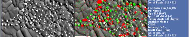
Fig.4 Auger image silver, copper system Sn · Ag · Cu · Bi (Pb-free solder)
Determining the elemental distribution in a depth profile
When analyzing a surface, the surface should not be contaminated. Therefore, the specimen analysis chamber is kept at an ultra high vacuum. Still, contamination attached to the specimen surface from the beginning is difficult to remove, so the ion source is used to irradiate ions onto specimen surface to eject the contamination. Using the ion source it is not only possible to clean the specimen surface, but also to cut away the specimen surface. So, by repeating the process of measuring the Auger spectrum and cutting away the material, the elemental distribution in depth direction can be obtained.
The Fig. 5 is the data of a solder ball specimen. As mentioned earlier, this data shows the elemental distribution in the depth direction. The horizontal axis corresponds to the depth direction, and the vertical axis represents the intensity of the Auger electrons of each element.
From this result, we see that oxygen and tin were detected on the specimen surface, so we know that the surface was covered with tin oxide. The thickness of the tin oxide layer influences the adhesive properties of the solder ball as well as characteristics such as electrical conductivity. Therefore, there are studies made to determine how the differences in manufacturing conditions and storage environments influence the thickness of the oxidized layer.
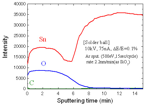
Fig.5 Depth profile of the different elements (solder ball)
Determining the chemical state
The solder ball characteristics mentioned above can be influenced by whether the oxidized layer is SnO2 or SnO, so it is important to measure the chemical state of the tin. JAMP-9500F equipped with an HSA can analyze the chemical state of various elements. Fig. 6 shows the standard spectra of SnO2, SnO and metal Sn.
When an atom is bonded with another atom, the peak position shifts, and the shape of the spectrum changes. In other words, the shape of the spectrum will vary depending on the chemical state of the elements.
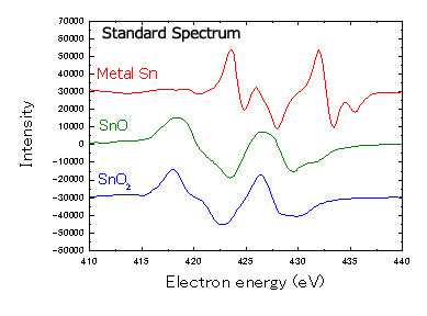
Fig.6 Standard spectrum Sn metal, SnO, of SnO2
By using standard spectra to mathematically separating the spectra obtained in Fig. 5, a depth profile distribution by chemical state can be obtained. The result of this chemical state analysis is shown in Fig. 7.
This result shows that the surface consists of SnO2 (tetravalent) and that divalent tin SnO exists in the interface with metallic tin.
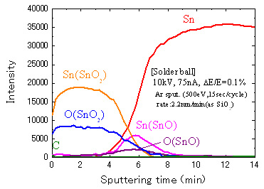
Fig.7 Depth profile of the different chemical state (solder ball)
Auger Microprobe challenging the nano-world
Since the Auger Electron Spectroscopy has a high performance electron optical system, and can collimate electron beams to very small, precise sizes, it is capable of analysis of very small areas, including structures on the order of 10nm (one-100,000th mm).
Because the composing elements and their chemical states in the uppermost surfaces and micro regions of a material often determine the physical properties of semiconductors, ceramics, and metals, the Auger Electron Spectroscopy fills an important role in surface analysis and very small area analysis, and is expected to increase an importance in the future.
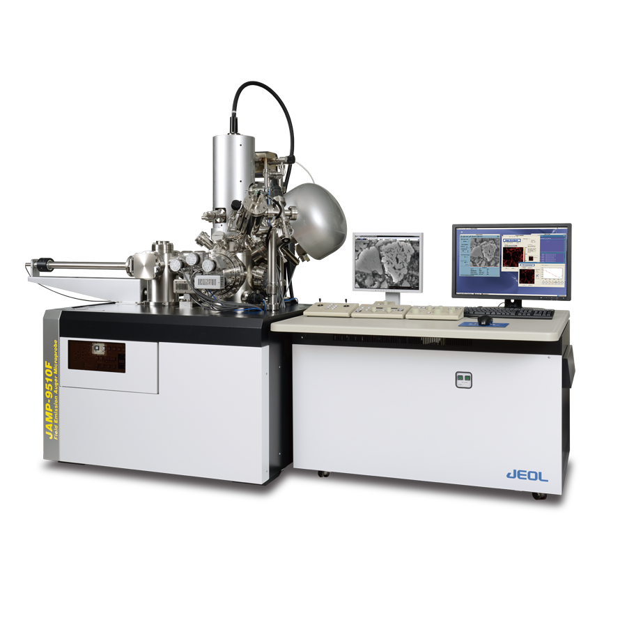
JEOL's "JAMP-9510F Field Emission Auger Microprobe" is a high specification Auger electron spectrometer with a hemispherical analyzer to provide high throughput analysis of the chemical bonding state at nano to micro areas, and a field emission electron gun also used for EPMA, because it can deliver a large, stable electric current. The highly precise eucentric specimen stage makes it possible to perform the previously-impossible analysis of insulators. This in combination with the floating type ion gun offers the versatility to handle any specimen, such as metals and insulation materials, to obtain composition information and chemical information.