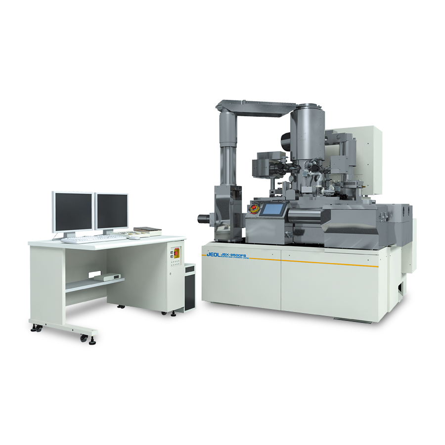
JBX-9500FS is a 100kV EB system that provides world-top-level throughput and positional accuracy among Spot beam lithography systems. This EB system can accommodate up to 300mmΦ wafer and up to 6-inch mask, thus responding to R&D and production in various fields, such as nanoimprint, photonic device and communication device.
Features
In addition to the maximum scan speed of 100MHz, JBX-9500FS achieves overlay accuracy of ±11nm, field stitching accuracy of ±10nm and positional accuracy within field of ±9nm when the field size is 1000µm×1000µm. Thus, JBX-9500FS is a 100kV EB system that provides world-top-level throughput and positional accuracy among Spot beam lithography systems.
Since JBX-9500FS employs Beam positioning DAC of 20bits and Scan DAC of 14bits, higher-resolution scan step of 0.25nm is obtained for writing data increment of 1nm, thus reproducing more precise writing data.
Its high scan speed up to 100MHz enables JBX-9500FS to maintain short scan steps at large-current writing, thus enhancing throughput even when high-precision pattern writing is required.
World-top-class positional accuracy is achieved by LBC (laser beam control) that provides the high-resolution, minimum beam positioning step of 0.15nm (λ/4096).
Furthermore, a unique auto calibration function (automatic correction function) developed by JEOL achieves highly reliable, stable pattern writing for a long period of time. Timing of auto correction can be set for each field or each pattern. This function is very effective for a long period writing without an operator, for example at weekends or consecutive holidays.
JBX-9500FS can accommodate up to 300mmΦ wafer and up to 6-inch mask, thus responding to R&D and production in various fields, such as nanoimprint, photonic device and communication device. Adding the material cassette transfer system (option) enables this EB system to load up to 10 cassettes.
The use of Fine Pitch Control Program (field size fine modulation program) enables JBX-9500FS to fabricate a chirped-period grating such as a DFB laser.
Introduction results
Over more than 40 years, JEOL has delivered a great deal of EB systems to research institutions and production lines in Japan and overseas.
Specifications
| Electron gun | ZrO/W Shottky type |
|---|---|
| Writing method | Spot beam, Vector scan, Step & repeat |
| Acc. Voltage | 100kV |
| Material size | Material size (possible to load): Up to 300mmΦ wafer, Up to 6-inch mask, Micro sample of any size |
| Maximum field size | 1000µm×1000µm |
| Stage movement range | 260mmX240mm |
| Stage control unit | 0.15nm(λ/4096) |
| Overlay accuracy | ≦±11nm |
| Field stitching accuracy | ≦±10nm (1000µm×1000µm field) |
| Positional accuracy within field plane | ≦±9nm(1000µm×1000µm field) |
| Beam positioning DAC | 20bit |
| Scan speed | Up to 100MHz |
More Info
Are you a medical professional or personnel engaged in medical care?
No
Please be reminded that these pages are not intended to provide the general public with information about the products.