JSM-IT710HR
Scanning Electron Microscope
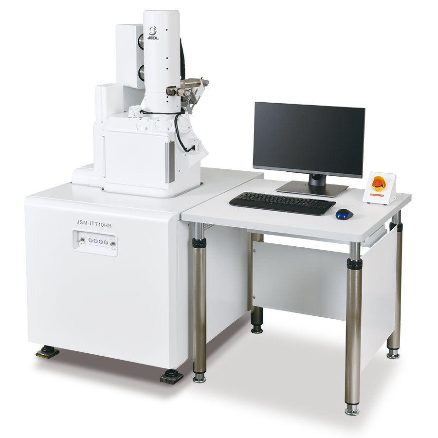
Clear visibility promotes new discovery
Nowadays, not only resolution and analytical performance on the nanometer order, but also throughput in data acquisition are considered important. The newly born JSM-IT710HR is the fourth-generation model of JEOL's HR* series, which is based on the theme of "SEM that allows anyone to easily take high-resolution images.
The JSM-IT710HR makes users want to pursue beyond what has been seen, due to ease of operation with enhanced automatic functions and improved observation performance from a new detector.
*HR=High Resolution
Features
Product video
I can see it, I want to see it more
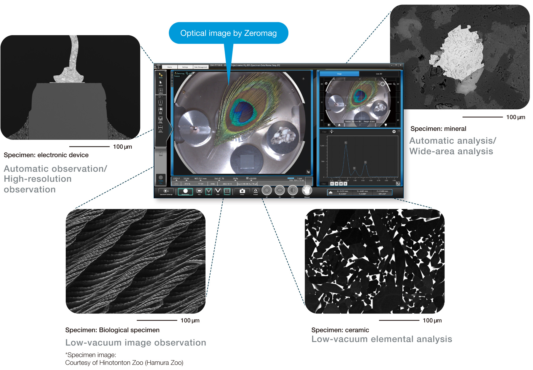
1. The SEM image is visible in conjunction with the optical image.
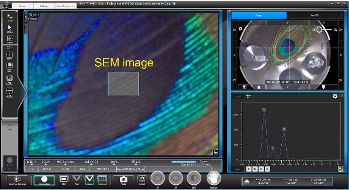
Specimen: courtesy of Hino Tonton ZOO (Hamura Zoo)
2. The image is seen better due to the high resolution electron gun.
I can see it, I want to see it more
Charge reduction
Low vacuum
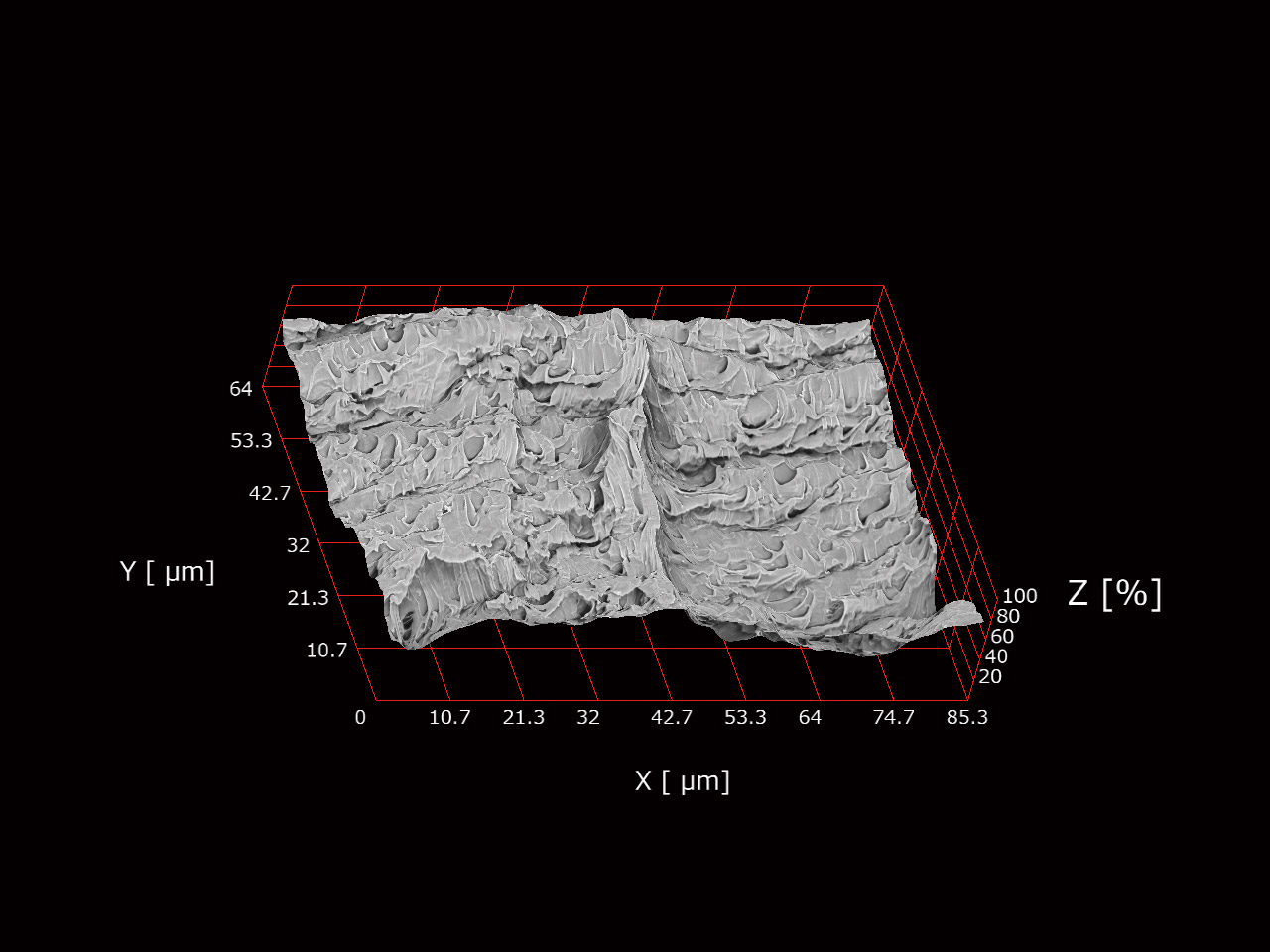
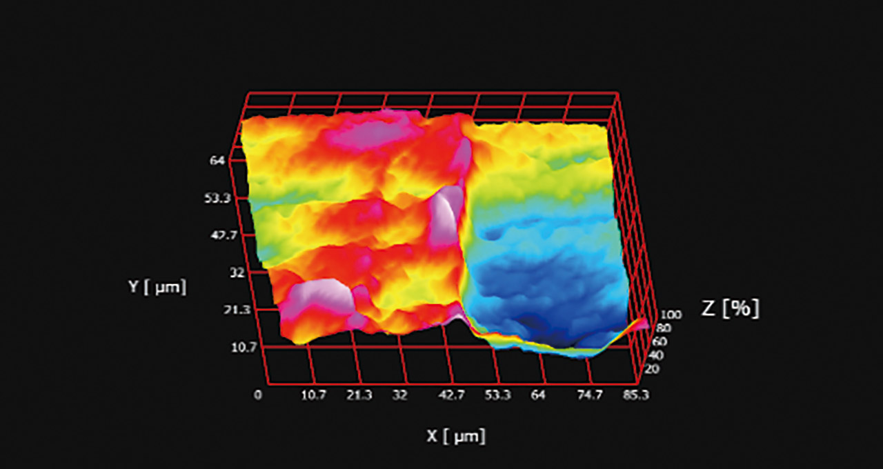
3D observation
Multi-segment detector
Elemental information
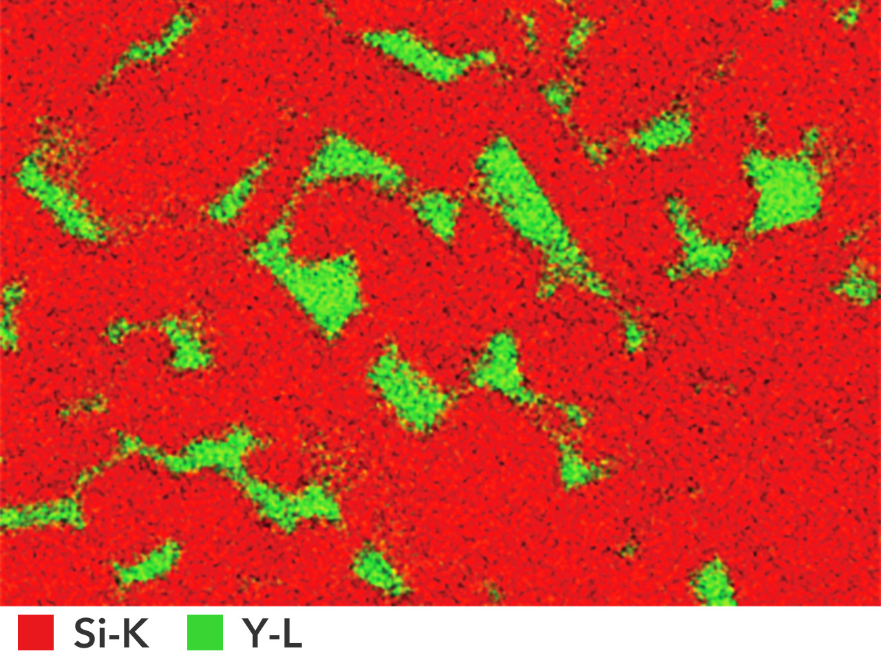
EDS※
Crystal structure analysis
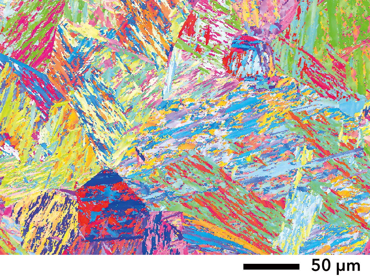
EBSD※
※optional
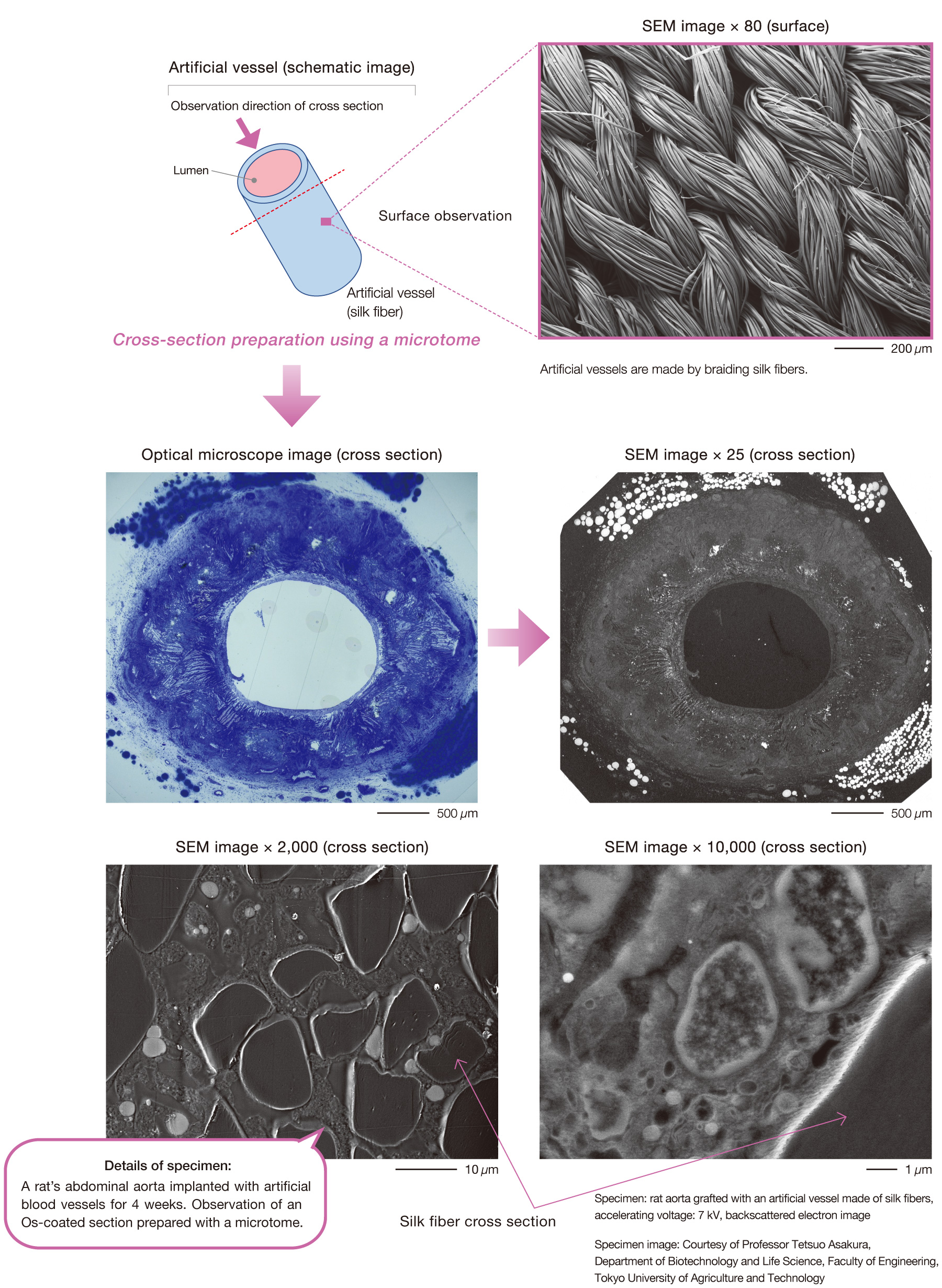
Charge reduction
Specimen: Courtesy of Prof. Tetsuro Asakura, Department of Biotechnology and Life Science, Tokyo University of Agriculture and Technology
Crystal structure analysis
Specimen: Courtesy of Prof. Kaneaki Tsuzaki, National Institute for Material Science (NIMS)
New functionality
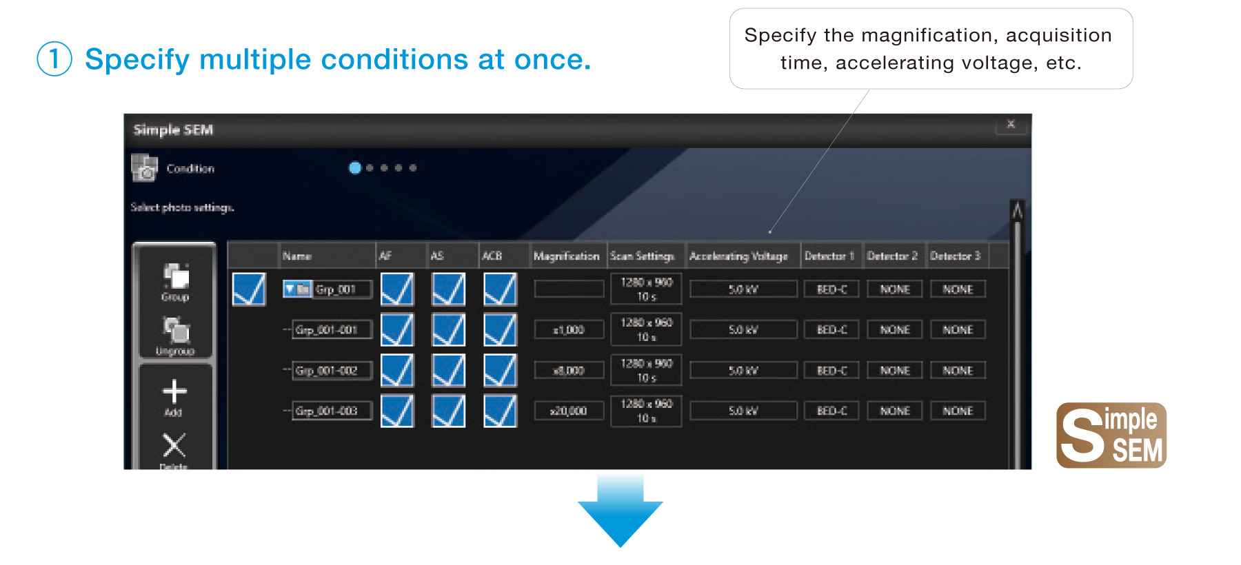
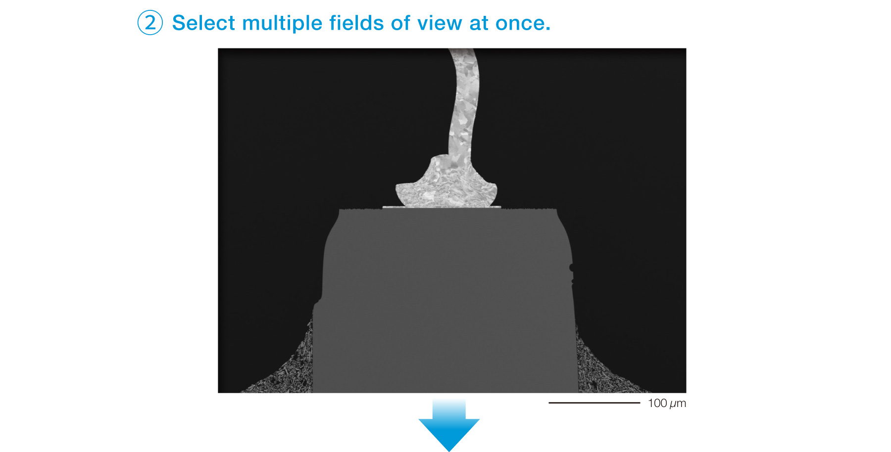
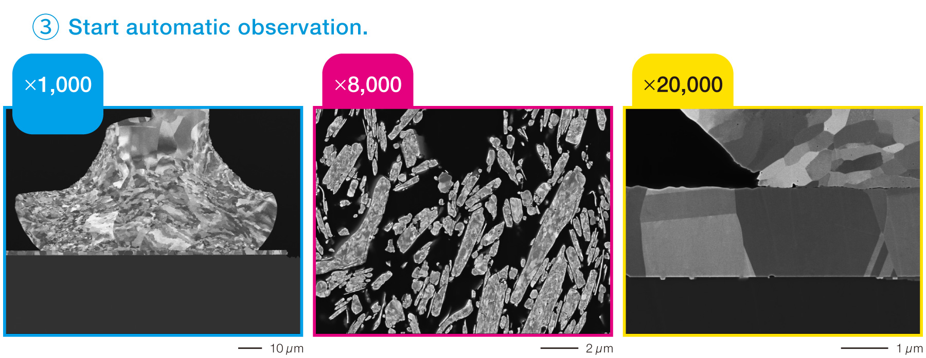
Automatic Observation:Simple SEM/EDS
Simple SEM function enables automatic measurements by registering multiple conditions at once. Simple
This improves the efficiency of routine work.
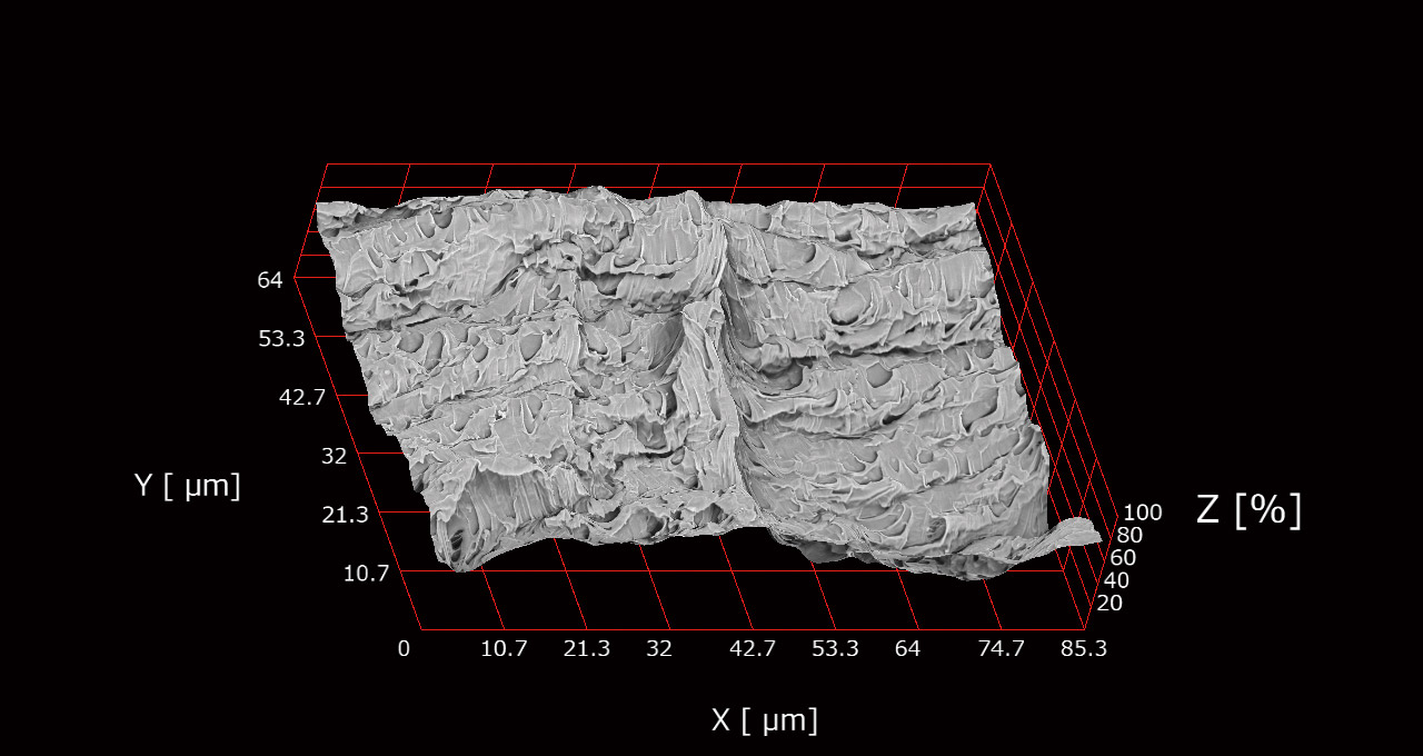
Live 3D: constructs 3D image on the spot
Imaging is possible at a low magnification with a little distortion, due to the out-lens objective lens.
Images acquired using the Quadrant detector

Specimen: Fracture surface of plastic
Live 3D image
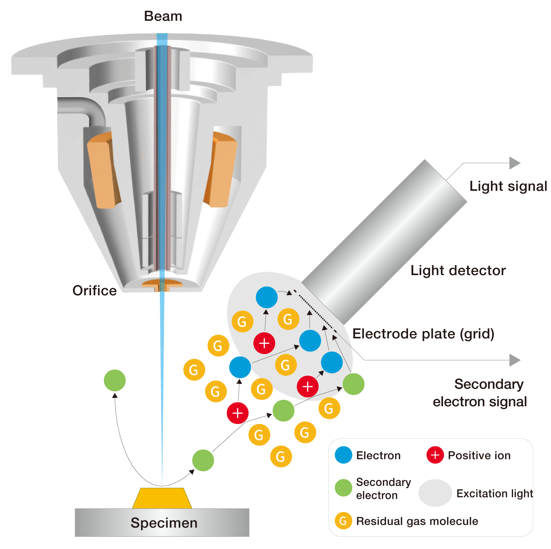
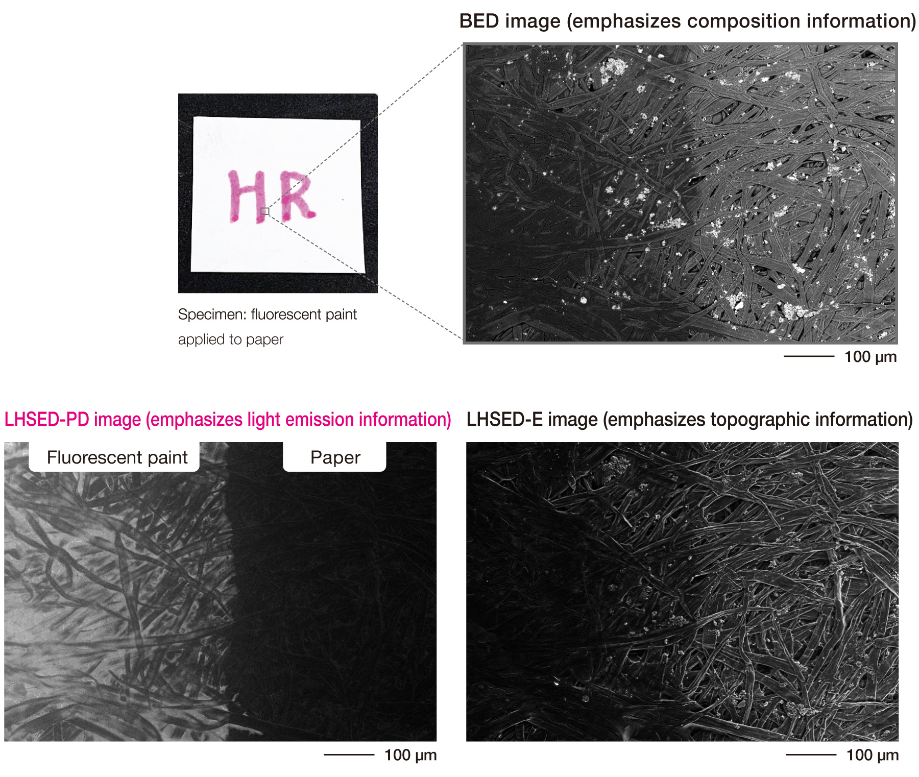
New Low Vacuum Hybrid Secondary Electron Detector (LHSE) ※Optional function
The LHSED, a new low-vacuum detector, enables observation while switching between images containing light emission information and topographic images.

LHSED Features
- Improved quality of low vacuum secondary electron live image
- Acquisition of light emission information
- Switching between topographic and light emission information images
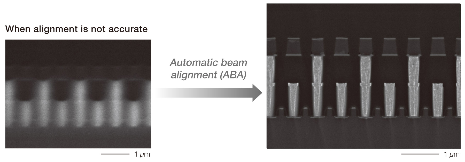
Schottky FE electron gun stability has been enhanced more than 4 times compared to the previous models
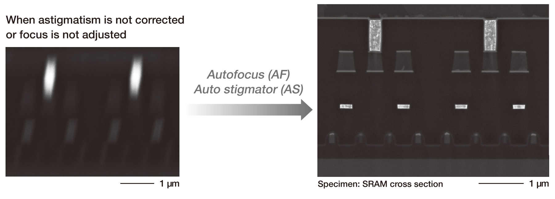
Automatic Beam Adjustment
JSM-IT710HR does not require complicated manual adjustment and provides automatic adjustment from axis alignment to astigmatism correction and focusing.
Secondary Electron Detection System
Secondary electron detector
(SED)
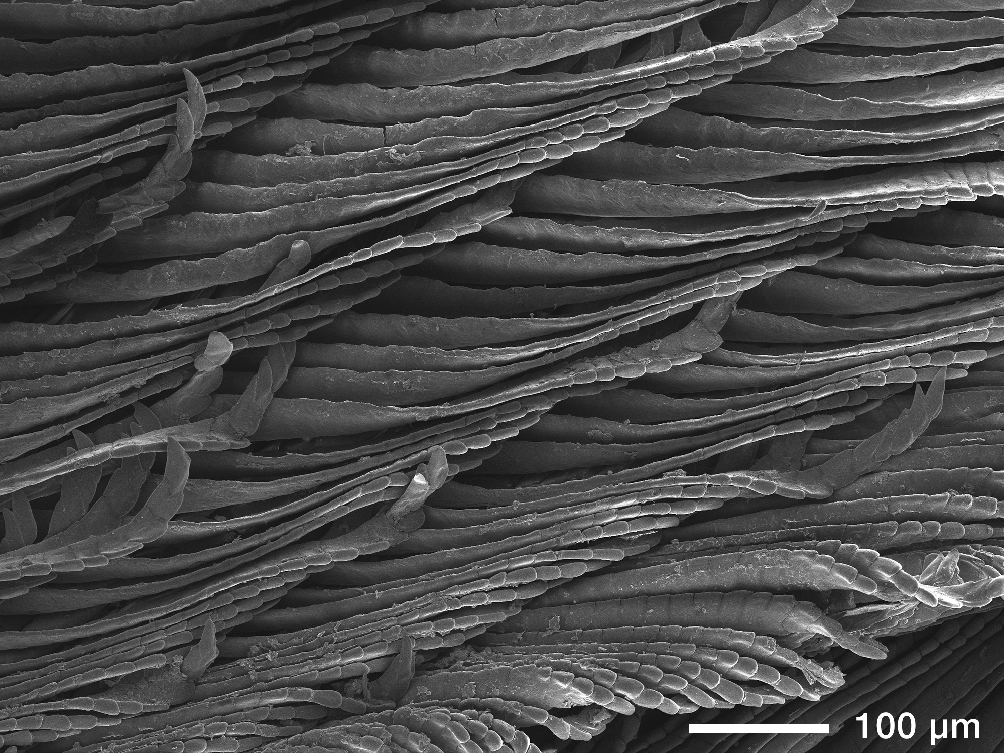
Specimen: Feather of peacock*
*Specimen image: Courtesy of Hinotonton Zoo (Hamura Zoo)
Low vacuum secondary electron detector
(LVSED/LHSED)
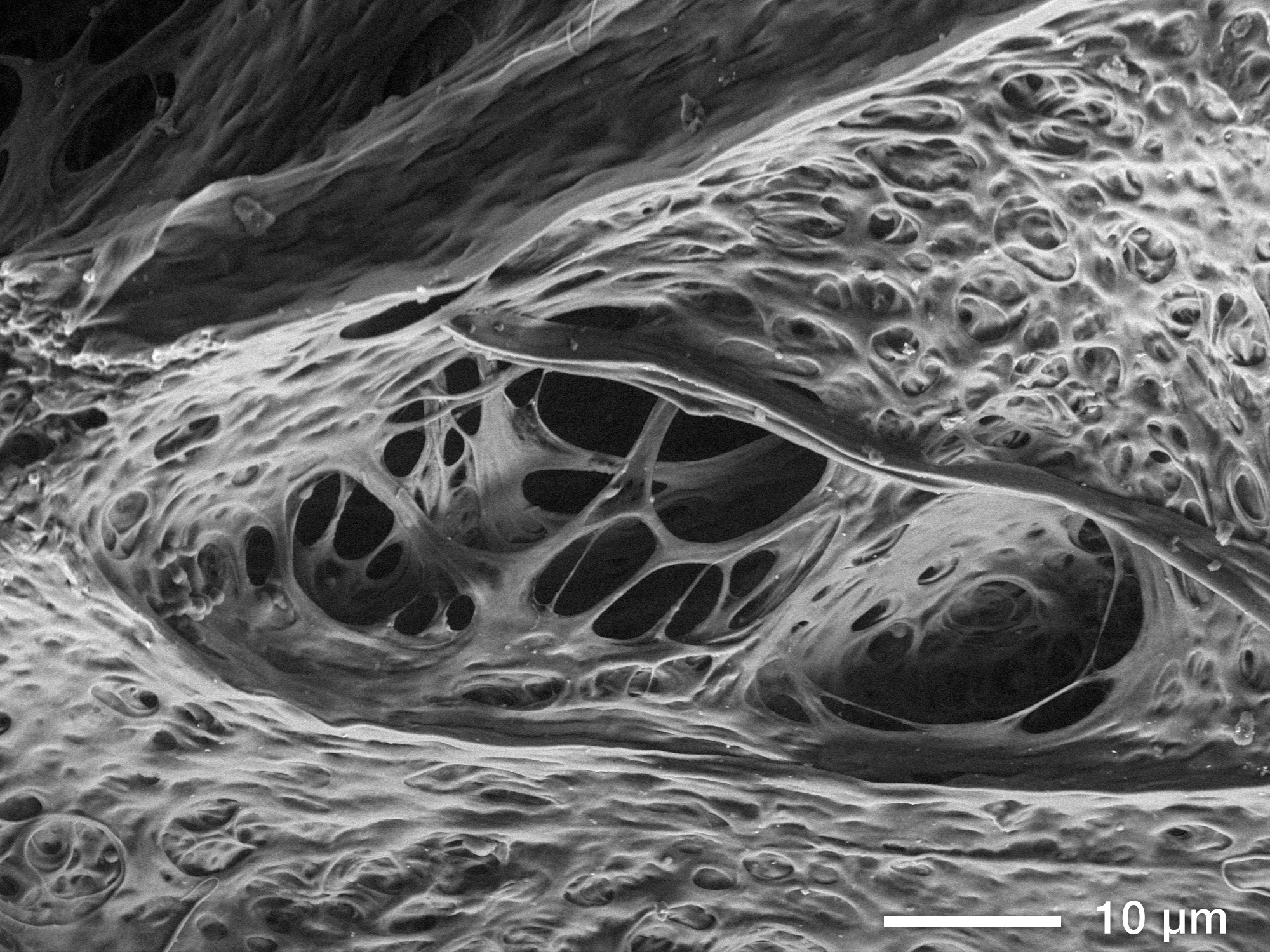
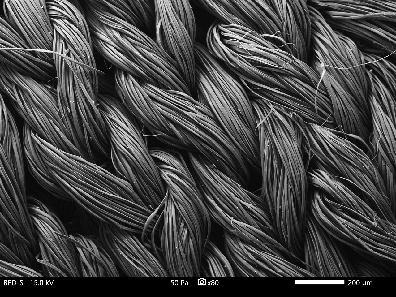
Specimen: cellulose microfiber
Both High Resolution and Large Current
The Schottky field emission gun used in the JSM-IT710HR enables high-resolution observation and analysis because the electron gun is integrated with the condenser lens to create large currents while maintaining a small probe.
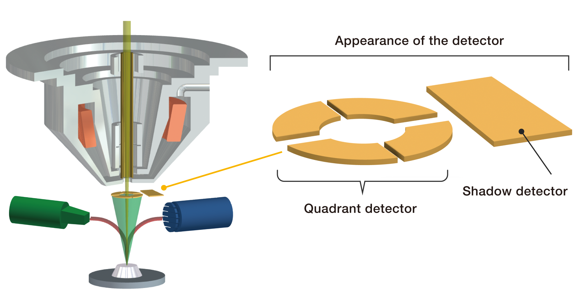
Backscattered Electron Detection System
The new multi-segmented backscattered electron detector acquires backscattered electron images from four directions at once so that a simple 3D image can be created and displayed live, in real-time.
Every Analysis Starts with Zeromag
Zeromag's optical image simplifies navigation.
SEM images can be linked to optical images for easy observation, analysis, and automated measurements.
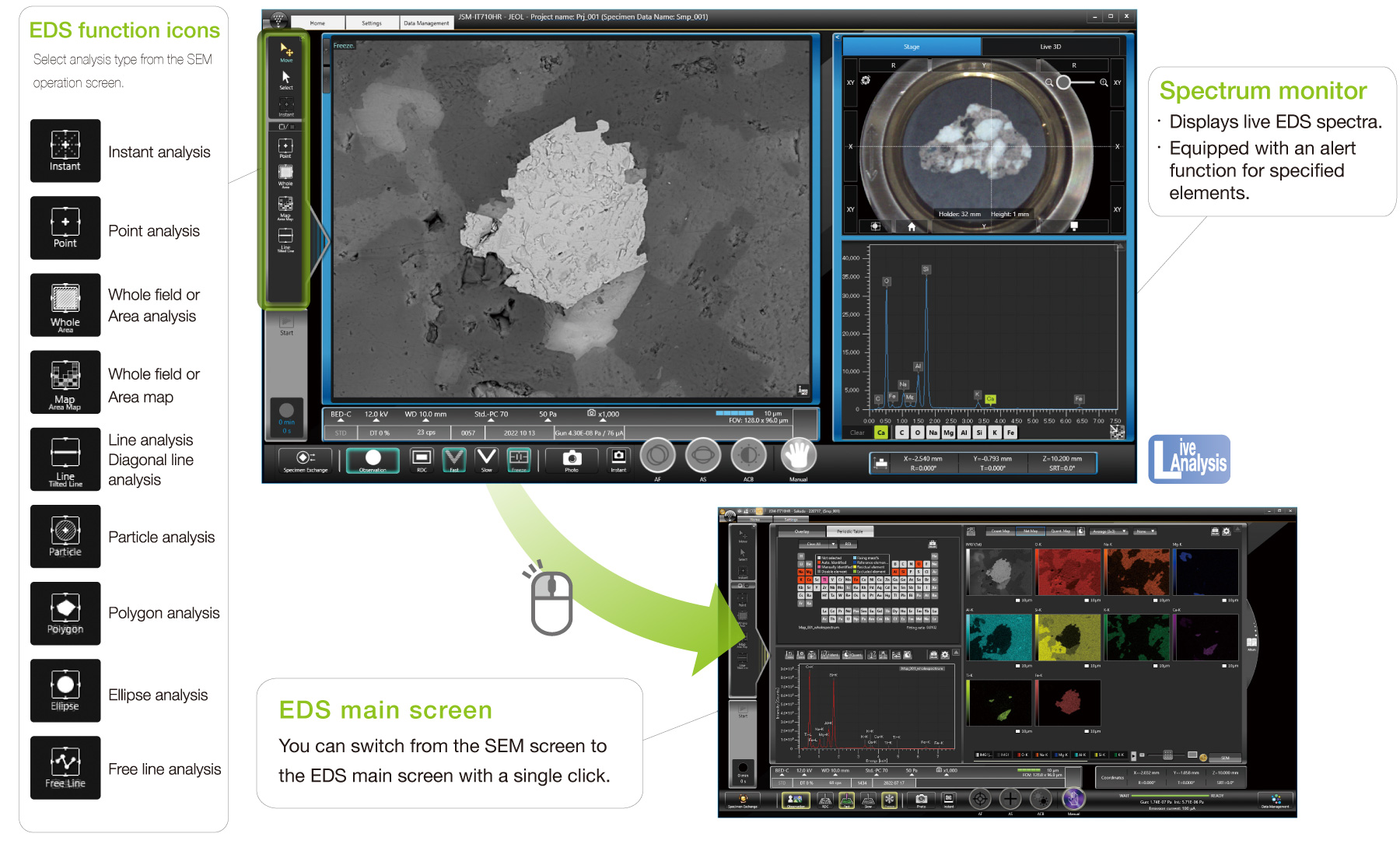
EDS Integration
JEOL manufactures and sells not only SEMs but also EDS.
Fully embedded EDS with SEM for simplified workflow, operation and data management.
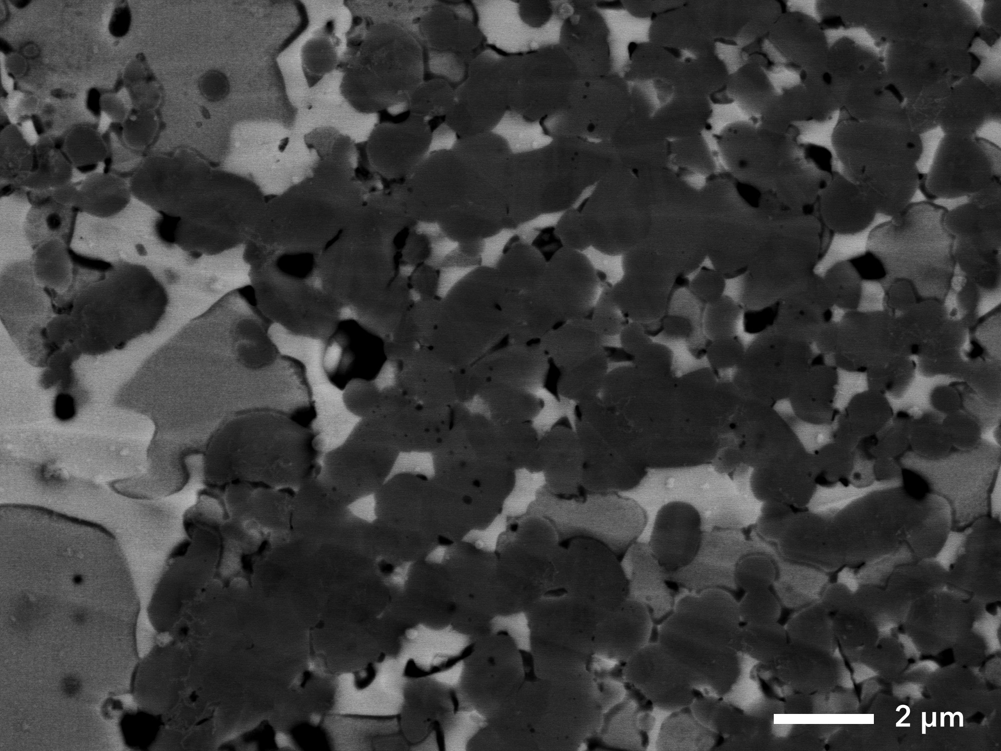
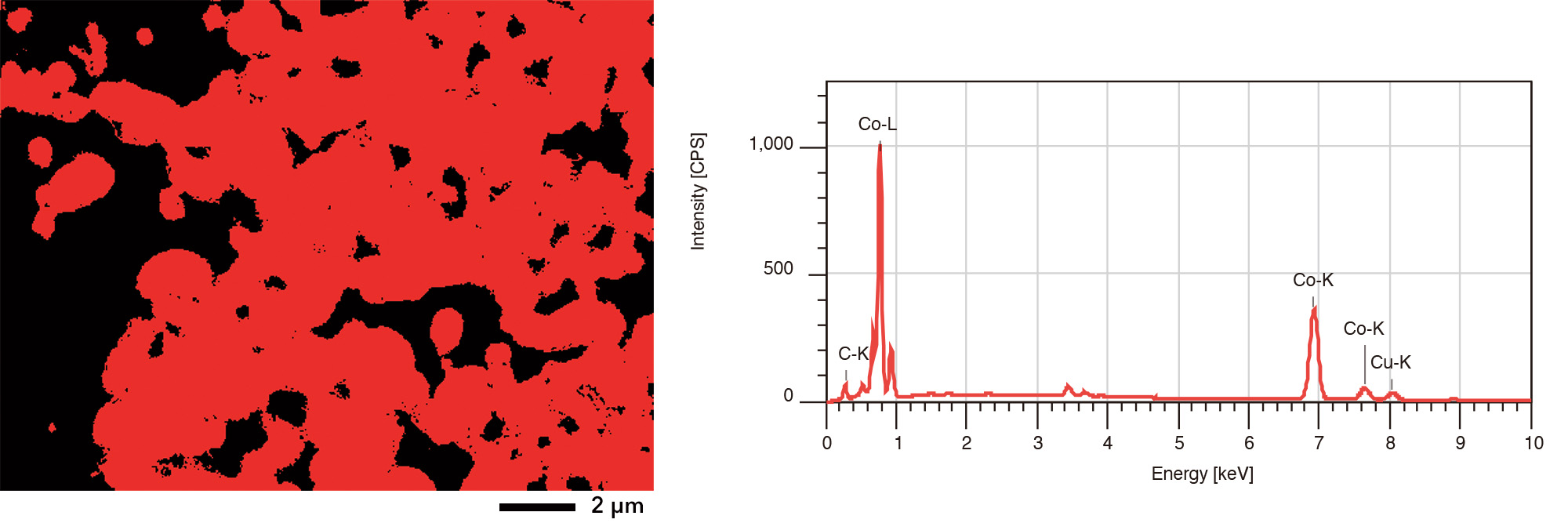
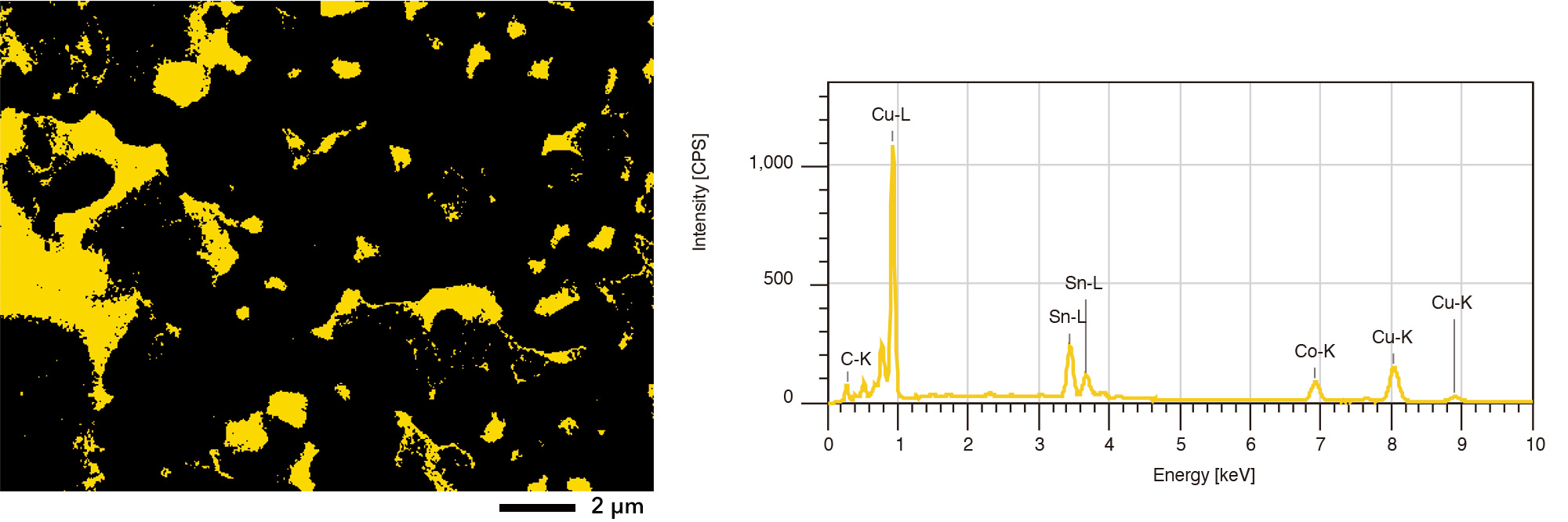
Phase Analysis
JEOL’s EDS system supports a new phase analysis function. Phase maps can be created from map data set.
Backscattered electron image
Phase mapping (Overlay of multiple phases)
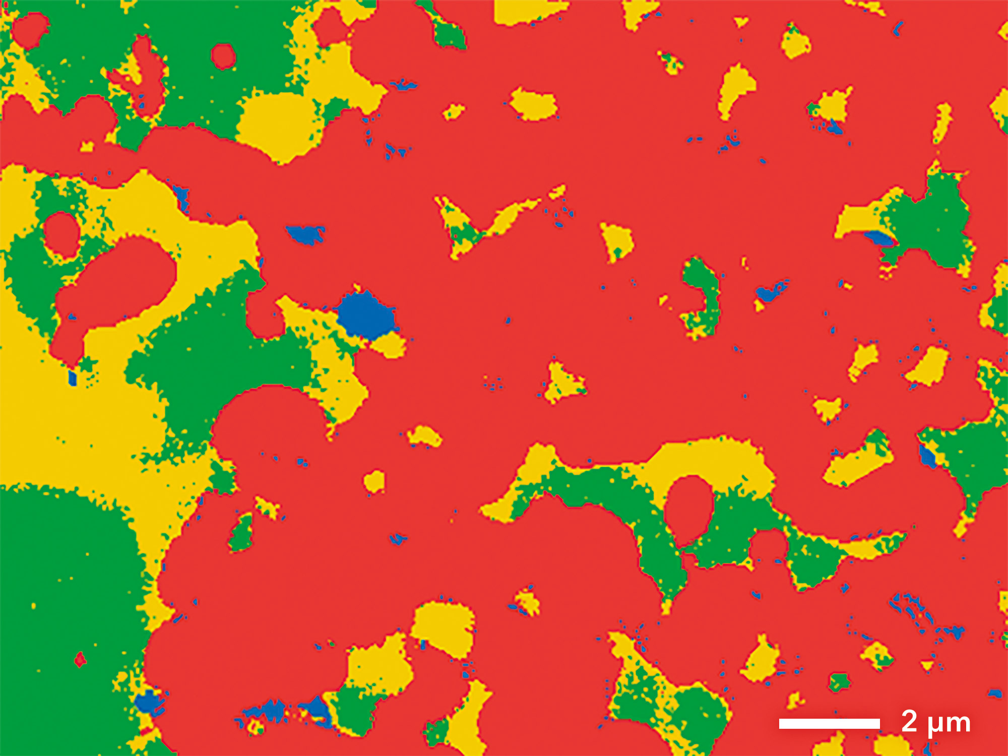
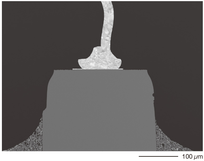
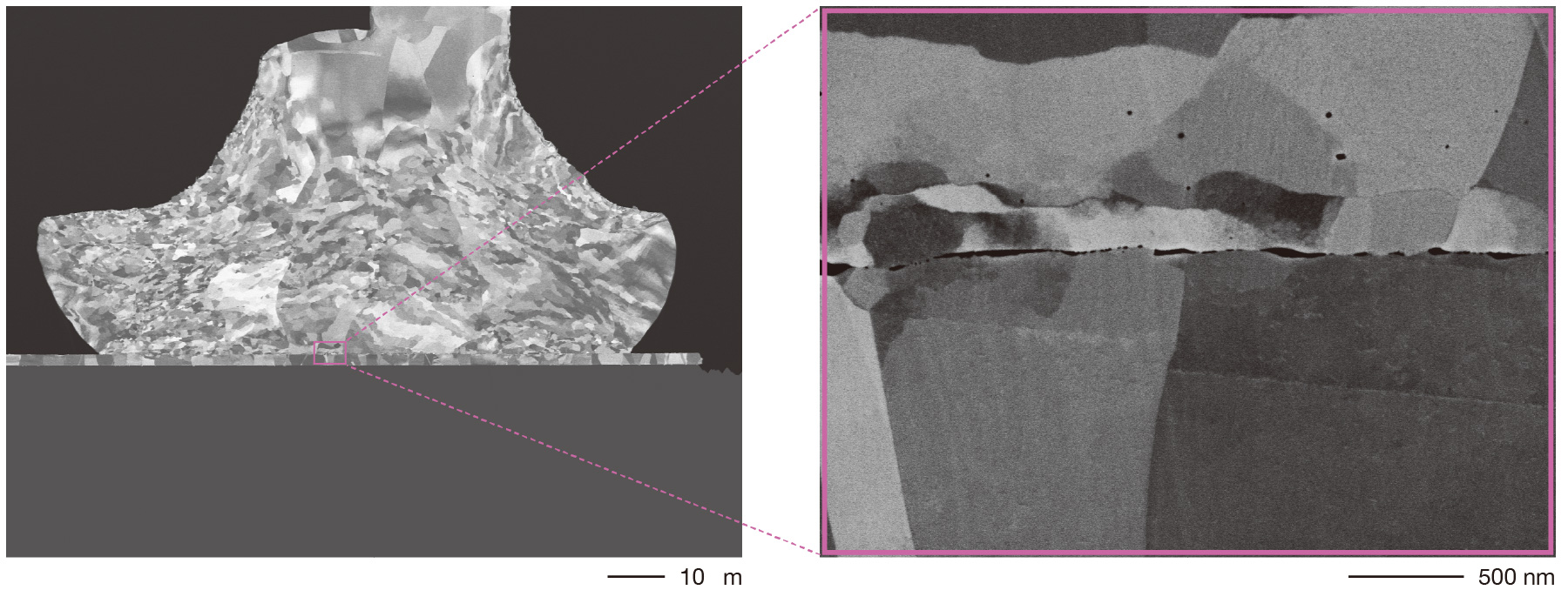
Specimen: cross section of a cutting tool for precision machining
Phase analysis indicates component difference between Co, Cu and Sn rich areas.
Co area: 68.15%
CuSn (CuRich) area: 16.25%
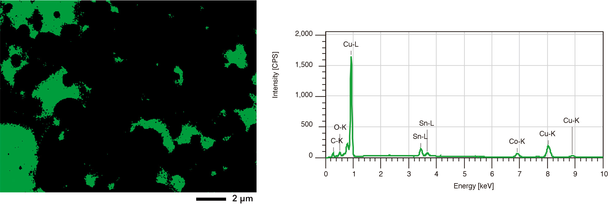
CuSn (SnRich) area: 14.54%
Specifications
Please refer to our product catalogue.
Catalogue Download
JSM-IT710HR Scanning Electron Microscope
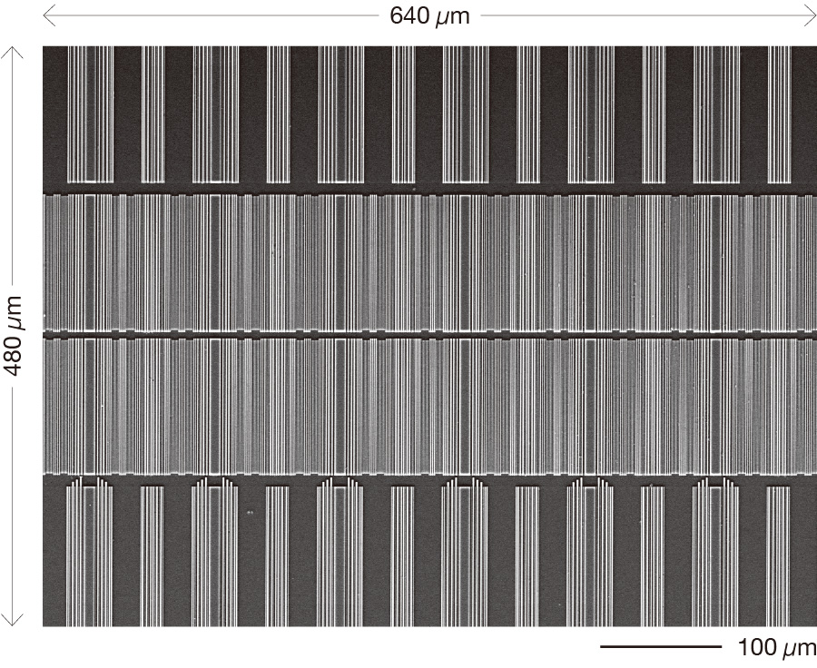
Application
Electronic Devices
Applicable features of JSM-IT710HR: high r esolution, high contrast, wide-ar ea observation
LED
Clear observation of a nanovoid at the junction interface of an electronic device
Specimen: LED cross section prepared using CP*
Magnification: ×250 (top), ×1,000 (bottom left), ×40,000 (bottom right)
Accelerating voltage: 5 kV
*CP: CROSS SECTION POLISHER™
Wiring pattern
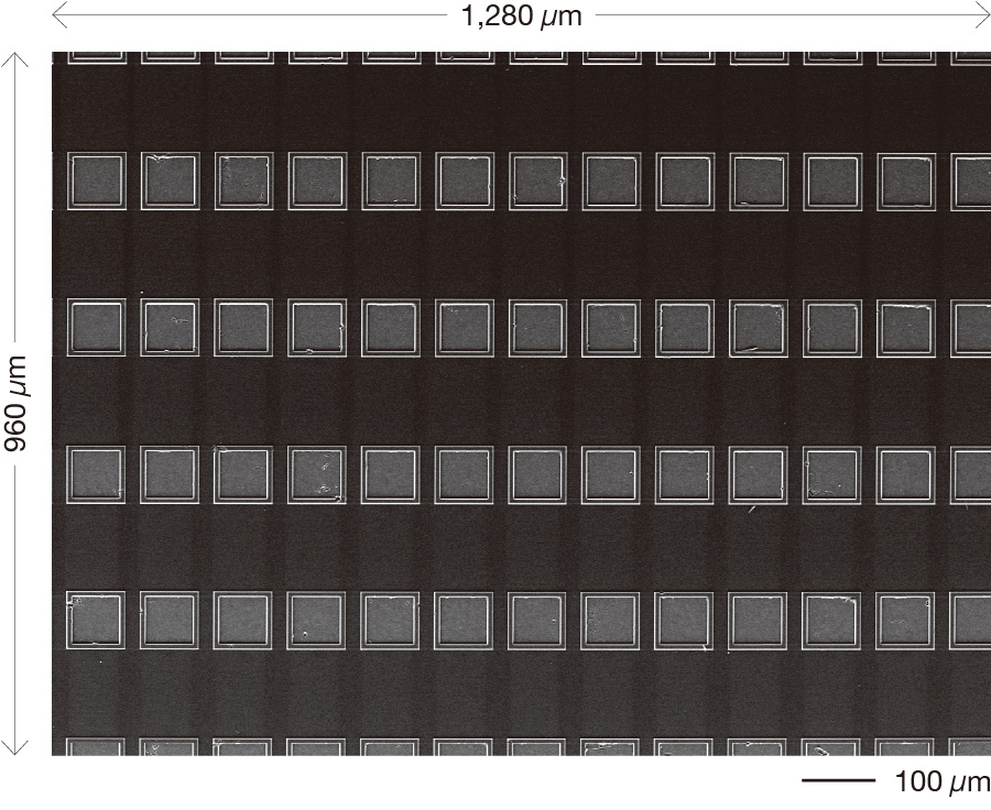
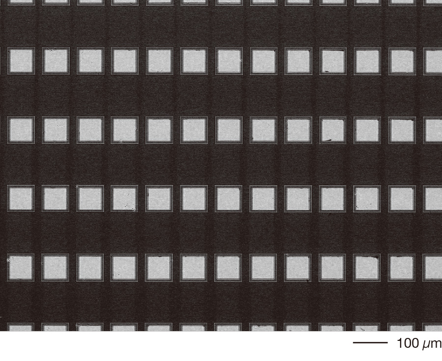
Using the low-vacuum function to observe a wide area of the wiring pattern surface
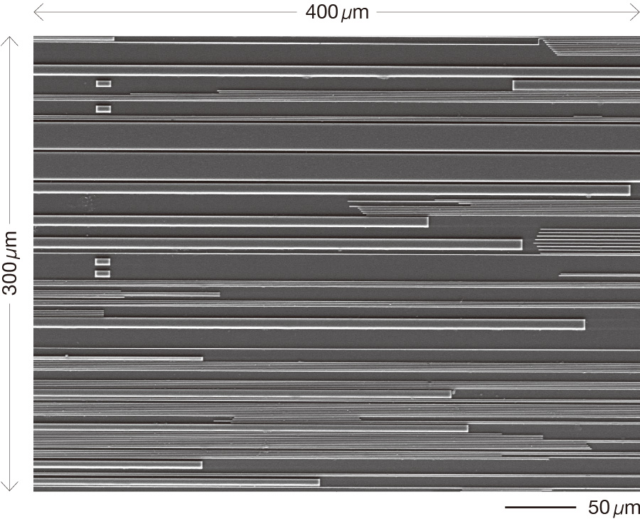
Specimen: wiring pattern surface, magnification: ×200 (left), ×300 (right), vacuum pressure: 70 Pa, accelerating voltage: 15 kV
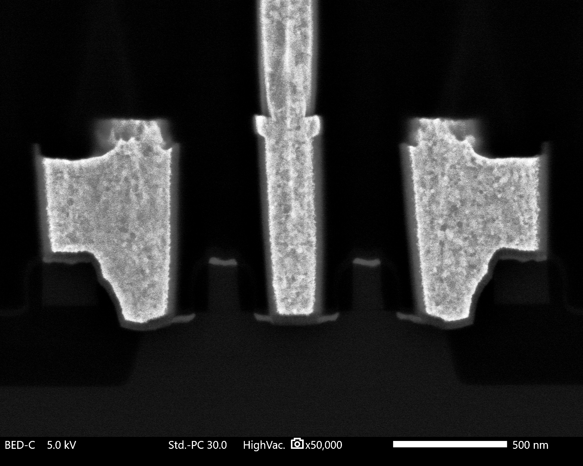
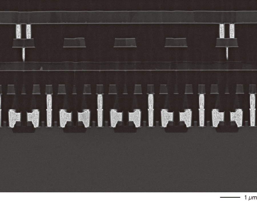
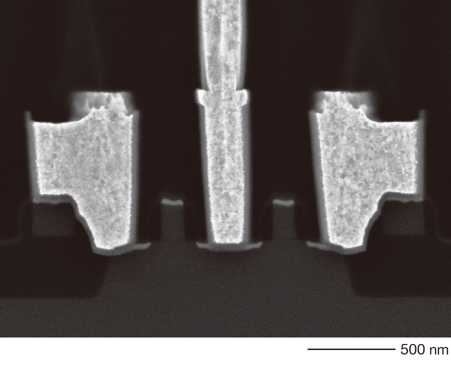
SRAM
High-resolution EDS map
Specimen: SRAM cross section prepared using CP
Magnification: ×10,000 (top), ×50,000 (bottom)
Accelerating voltage: 5 kV (SEM), 7 kV (EDS)
Backscattered electron image
EDS map
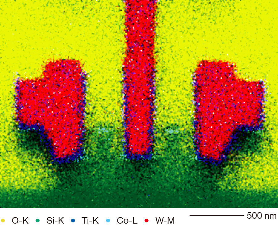
Al bonding pad
By acquiring both low-vacuum secondary electron images and backscattered electron images at the same time, the topographic information and composition information of a wide specimen surface area can be acquired.
Low-vacuum secondary electron image
Low-vacuum backscattered electron image
Specimen: bonding pad surface, magnification: ×100, vacuum pressure: 70 Pa, accelerating voltage: 15 kV
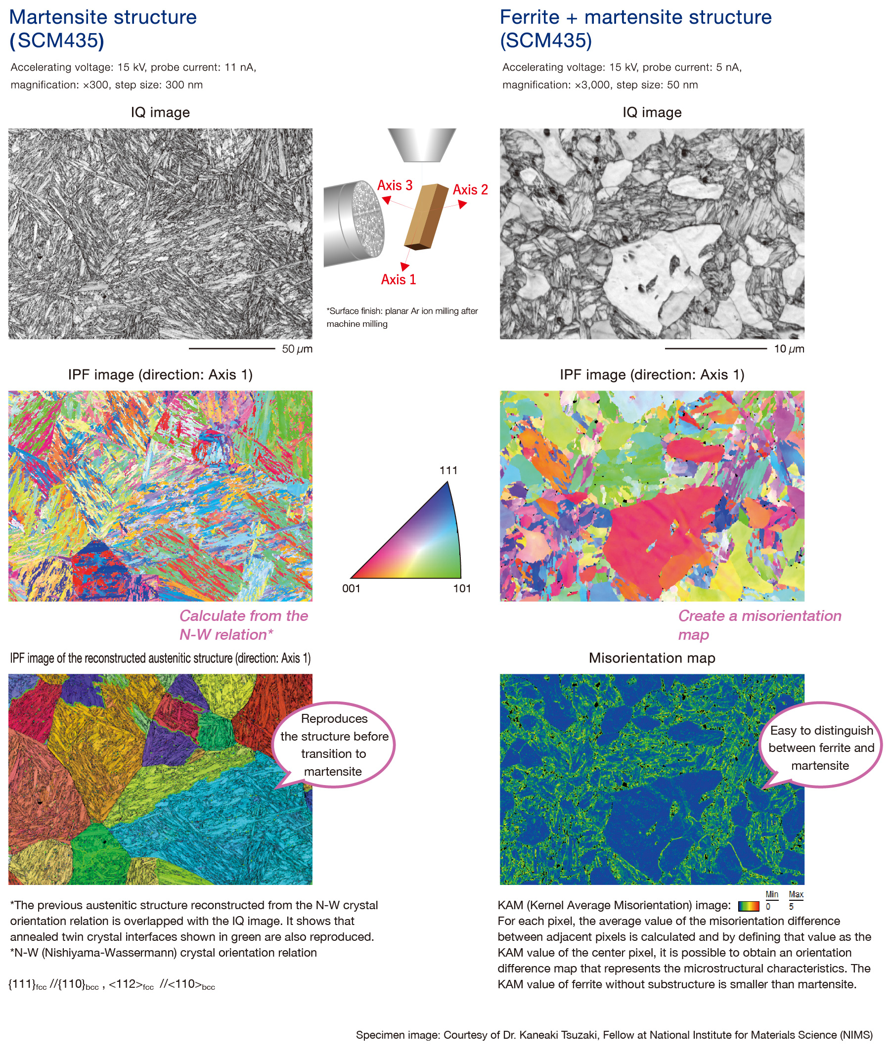
Steel
Applicable features of JSM-IT710HR: optical system suitable for EBSD analysis (Schottky field emission gun and out-lens objective lens)
Energy and Ceramics
Applicable featur es of JSM-IT710HR: analysis capabilities and low-vacuum function
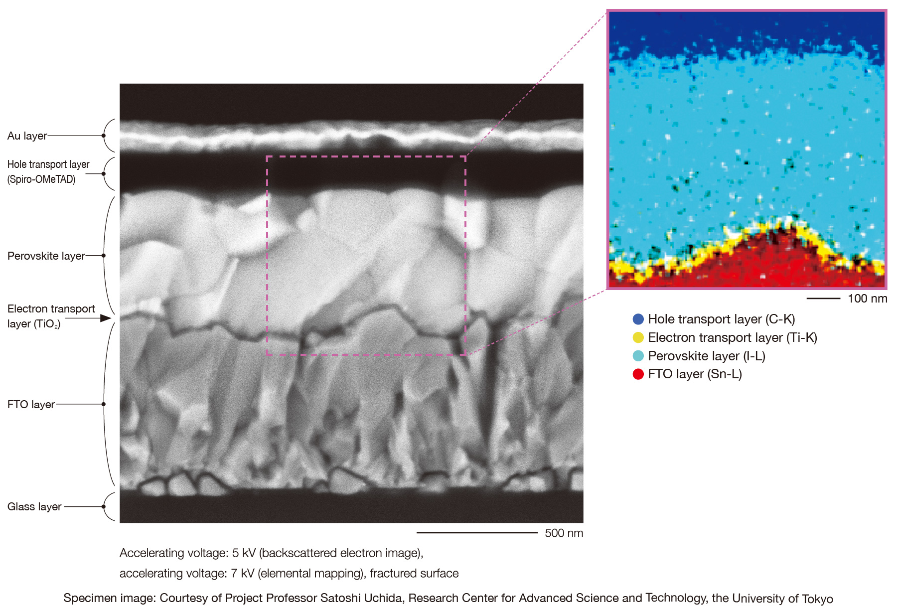
Perovskite solar cell substrate
High-accuracy analysis of nano-scale layers in the solar cell substrate
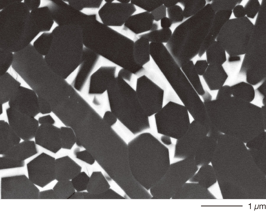
Ceramic substrate (Si3N4)
Low-vacuum function enables elemental analysis of non-conductive specimens.
Low-vacuum backscattered electron image
Low-vacuum elemental map
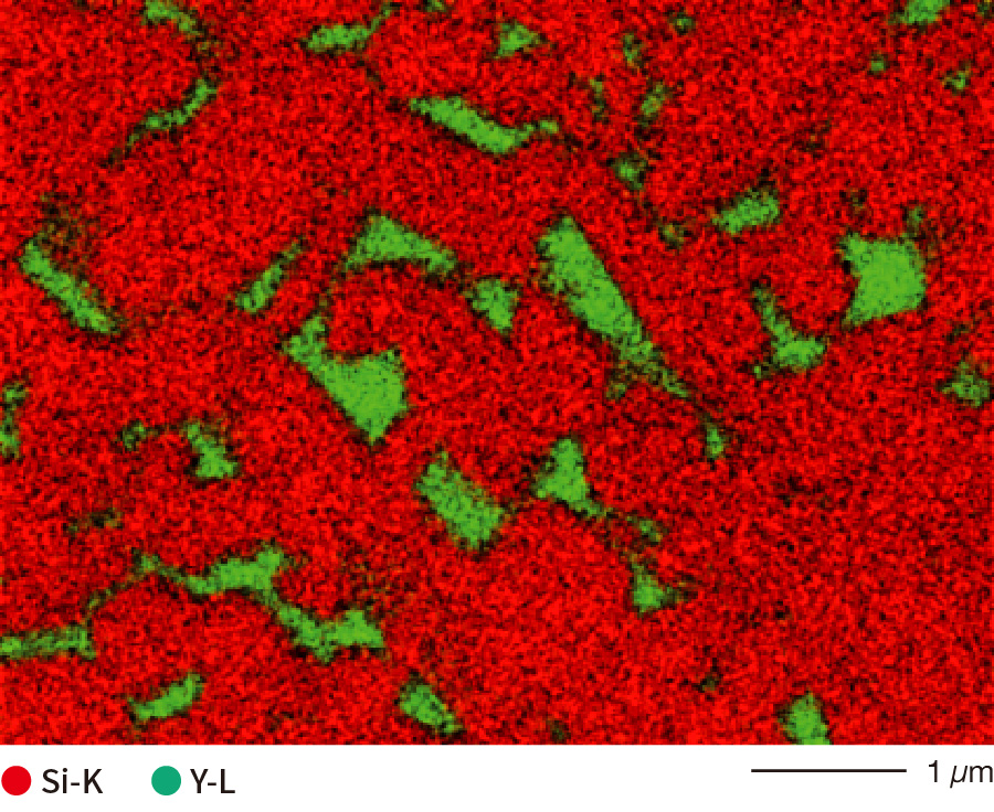
Accelerating voltage: 5 kV, low-vacuum elemental mapping (30 Pa), Machine milled surface of Si3N4 substrate*
*Surface finish: planar argon ion milling after machine milling
Soft Material and Life Science
Applicable features of JSM-IT710HR: low accelerating voltage, low-vacuum functio n, and ultra-low magnification observation
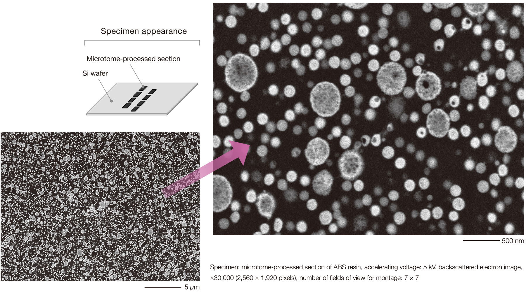
ABS resin
Even multiple images observed at a magnification of tens of thousands can be acquired with high accuracy and stable brightness.
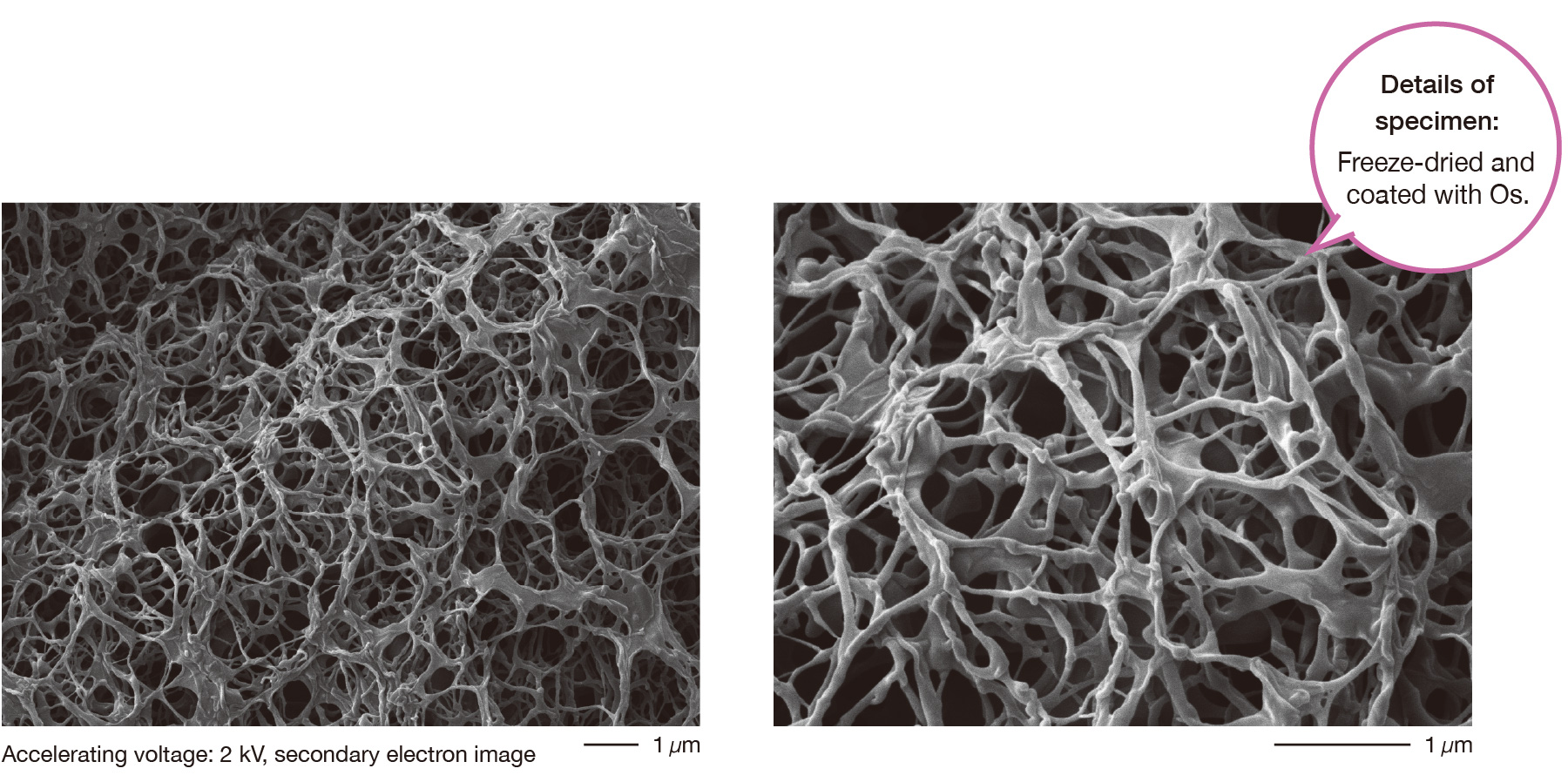
Gelatin
High-brightness, high-resolution secondary electron image
Artificial vessel
Observing a biological specimen on a slide glass from low to high magnification
Related Products
Scanning Electron Microscope (SEM)
Specimen Preparation Equipment (CP)
More Info
Are you a medical professional or personnel engaged in medical care?
No
Please be reminded that these pages are not intended to provide the general public with information about the products.